Method and system for defect detection in manufacturing integrated circuits

a manufacturing integrated circuit and defect detection technology, applied in the field of integrated circuits, can solve the problems of many limitations, large cost of manufacturing facilities, and difficulty in small devices, and achieve the effect of fast and automated solutions

Active Publication Date: 2011-08-02
SEMICON MFG INT (SHANGHAI) CORP
View PDF10 Cites 6 Cited by
  • Summary
  • Abstract
  • Description
  • Claims
  • Application Information

AI Technical Summary

Benefits of technology

[0012]It is to be appreciated that various embodiments of the present invention provide many advantages over conventional techniques. According to certain embodiments, the present invention utilizes non-parametric statistical tools to identify sources for manufacturing defects. For example, an embodiment of the present invention uses the Kruskal-Wallis test to identify late latent defects. According to a specific embodiment, the present invention provides a fast and automated solution for identifying sources for defects. For example, data relating to the processing of semiconductor substrates are automatically collected and analyzed. In addition, it is to be appreciated the various embodiments of the present invention are compatible with existing and conventional techniques. There are other benefits as well.

Problems solved by technology

An IC fabrication facility can cost hundreds of millions, or even billions, of dollars.
Making devices smaller is very challenging, as each process used in IC fabrication has a limit.
Although fabless chip companies and foundry services have increased through the years, many limitations still exist.
For example, tools for detecting defects during the manufacturing process have are often inadequate.
Due to costs and other practical considerations, integrated circuits (or rather partially processed integrated circuits) are not tested at every processing step.
As a result, it is often difficult to isolate and identify the sources of manufacturing defects.
Unfortunately, these techniques are often inadequate.

Method used


Image

  • Method and system for defect detection in manufacturing integrated circuits
  • Method and system for defect detection in manufacturing integrated circuits
  • Method and system for defect detection in manufacturing integrated circuits

Examples


Embodiment Construction

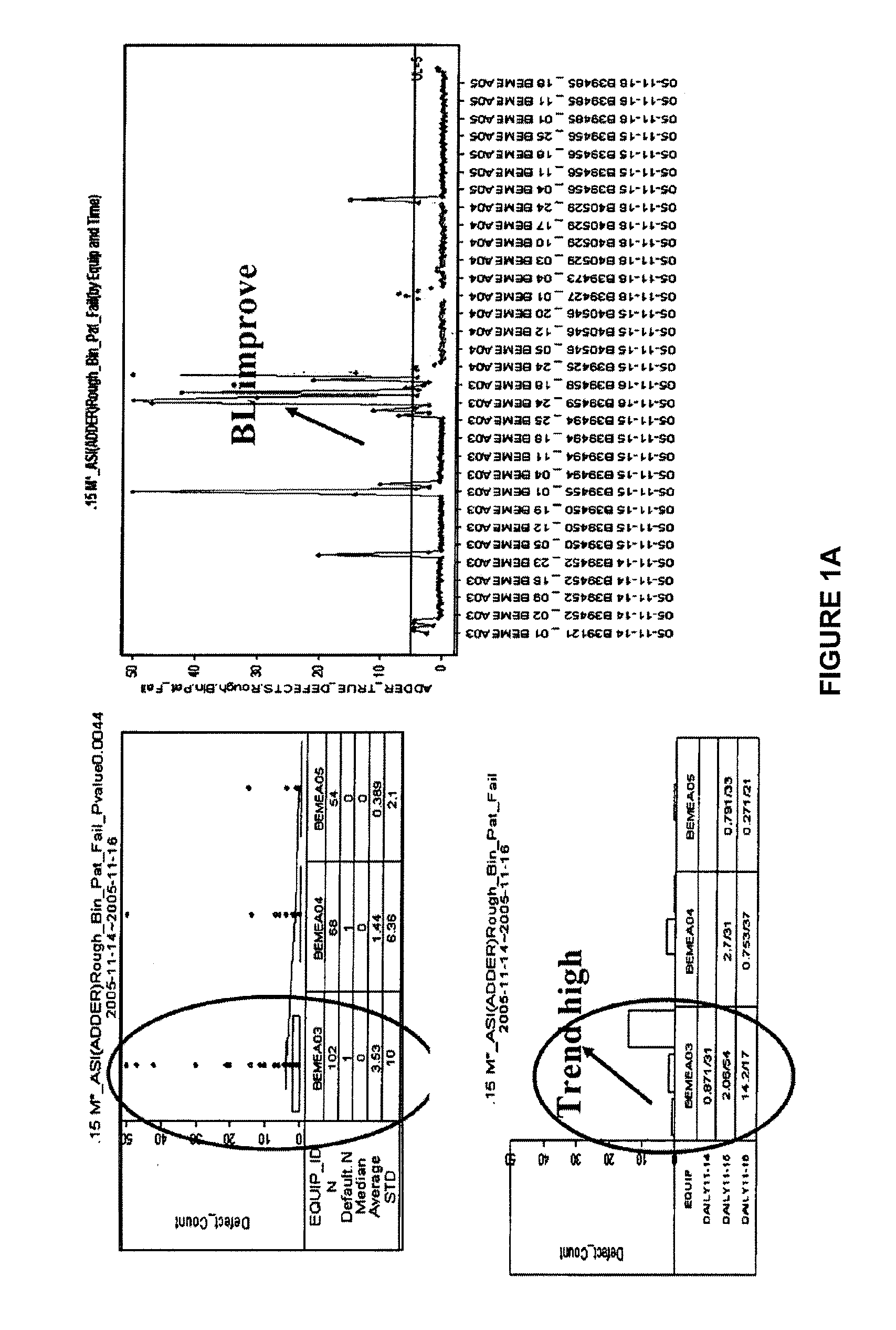
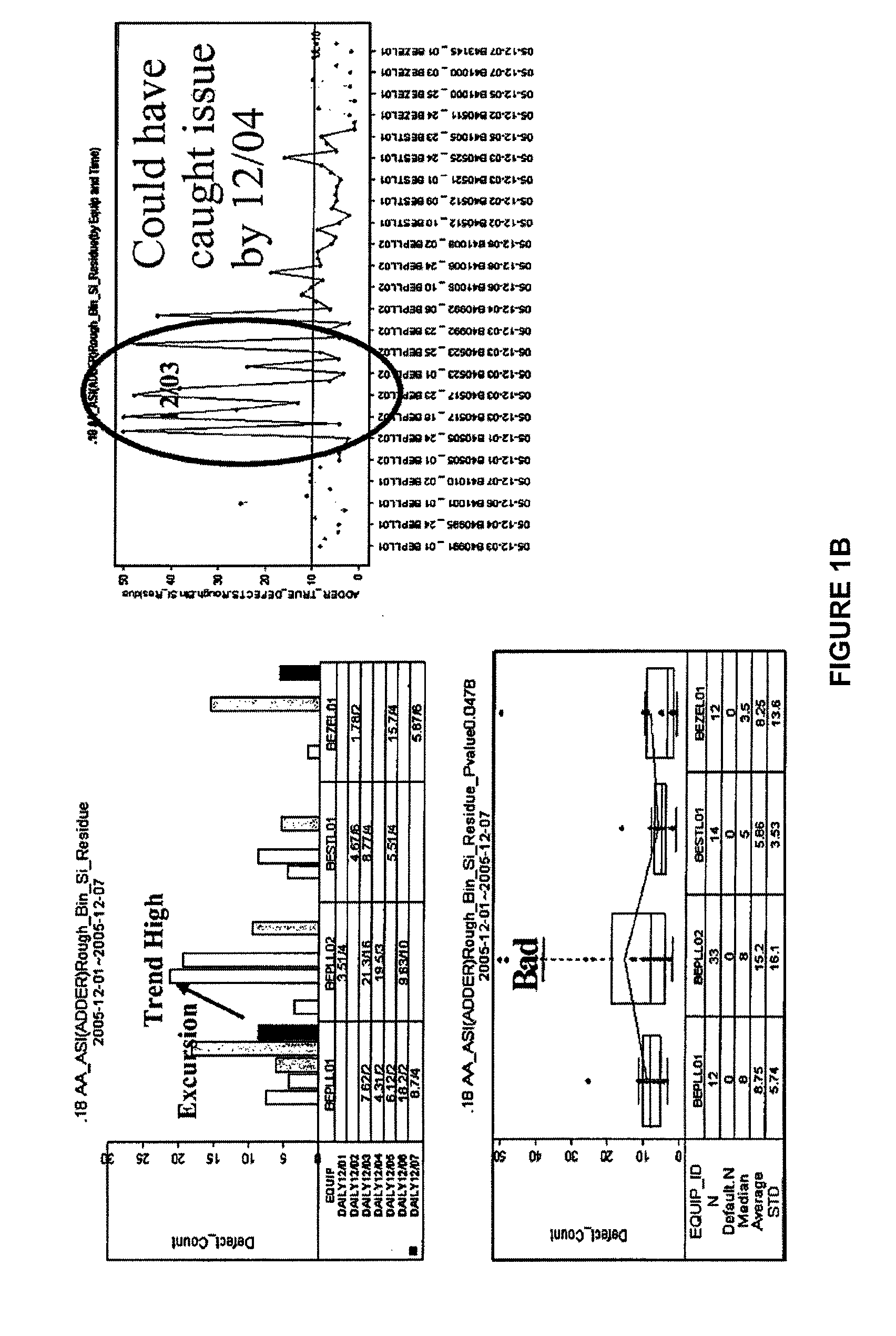
[0020]The present invention is directed to integrated circuits and their processing for the manufacture of semiconductor devices. More particularly, the invention provides a method and system for automated defect diction for the manufacture of integrated circuits. Merely by way of example, the invention has been applied to detecting defects using non-parametric statistical tools for the manufacturing of integrated circuits. But it would be recognized that the invention has a much broader range of applicability. For example, the invention can be applied to detecting defects in other manufacturing processes.

[0021]As explained above, detecting manufacturing defects and identifying the likely sources of manufacturing defects are important for the manufacturing of semiconductor wafers. In the past, various conventional techniques have been developed. Unfortunately, conventional techniques are often inadequate.

[0022]For example, one of the methods for identifying sources of defects has be...


PUM


Abstract

Method and system for defect detection in manufacturing integrated circuits. In an embodiment, the invention provides a method for identifying one or more sources for possible causing manufacturing detects in integrated circuits. The method includes a step for providing a plurality of semiconductor substrates. The method includes a step for processing the plurality of semiconductor substrates in a plurality of processing steps using a plurality of processing tools. The method additionally includes a step for providing a database, which includes data associated with the processing of the plurality of semiconductor substrates. The method further includes a step for testing the plurality of semiconductor wafers after the processing of the plurality of semiconductor substrates. Additionally, the method includes a step for detecting at least one defect characteristic associated with the plurality of the semiconductor substrates that have been processed. Moreover, the method includes a step for identifying a set of processing steps. For example, the set of processing step are possibly associated with the defect characteristic.

Description

CROSS-REFERENCE TO RELATED APPLICATIONS[0001]This application claims priority to Chinese Patent Application No. 200810040282.2, filed Jul. 2, 2008, commonly assigned, and incorporated herein by reference for all purposes.BACKGROUND OF THE INVENTION[0002]The present invention is directed to integrated circuits and their processing for the manufacture of semiconductor devices. More particularly, the invention provides a method and system for automated defect diction for the manufacture of integrated circuits. Merely by way of example, the invention has been applied to detecting defects using non-parametric statistical tools for the manufacturing of integrated circuits. But it would be recognized that the invention has a much broader range of applicability. For example, the invention can be applied to detecting defects in other manufacturing processes.[0003]Integrated circuits or “ICs” have evolved from a handful of interconnected devices fabricated on a single chip of silicon to milli...

Claims


Application Information

Patent Timeline
Patent Type & Authority Patents(United States)
IPC IPC(8): G06F19/00
CPCG05B19/41875G05B2219/32191G05B2219/32221H01L22/12G05B2219/11G05B2223/02Y02P90/02
Inventor LIN, PAUL KUANG-CHIZHANG, SOPHIA
Owner SEMICON MFG INT (SHANGHAI) CORP
Why Eureka
Try Eureka