Shaped MEMS contact

a contact and shaped technology, applied in the field of shaped mems contacts, can solve the problems of low cost, bulky switches, and not easily integrated with many radio frequency components, and achieve the effect of easy low-cost fabrication

Inactive Publication Date: 2011-03-15
THE UNITED STATES OF AMERICA AS REPRESETNED BY THE SEC OF THE AIR FORCE
View PDF2 Cites 0 Cited by
  • Summary
  • Abstract
  • Description
  • Claims
  • Application Information

AI Technical Summary

Benefits of technology

[0007]The present invention provides a low cost easily fabricated metallic electrical contact assembly especially suited for use in a radio frequency microelectromechanical switch.
[0018]It is another object of the invention to provide a microelectromechanical switch arrangement providing desirably low electrical contact resistance.
[0019]It is another object of the invention to provide a microelectromechanical switch arrangement providing desirable contact resistance to mechanical wear.
[0020]It is another object of the invention to provide a MEMS switch upper contact that is more easily cleaned by normal contact use wiping action.
[0022]It is another object of the invention to provide a MEMS switch upper contact that achieves a consistent wear pattern.

Problems solved by technology

Such solid state devices are often small and easily integrated with other radio frequency components but provide relative poor electrical performance.
In contrast the larger in size Macro switches offer relatively good electrical performance including isolation measuring greater than 70 decibels, insertion losses near 0.07 decibels and contact resistances of less than one ohm however such switches are bulky and not easily integrated with many radio frequency components.
Flat upper electric contacts are, however, not easily cleaned, have inconsistent wear patterns, and do not allow for switch operation at different areas on the contact surface.

Method used


Image

  • Shaped MEMS contact
  • Shaped MEMS contact
  • Shaped MEMS contact

Examples


Embodiment Construction

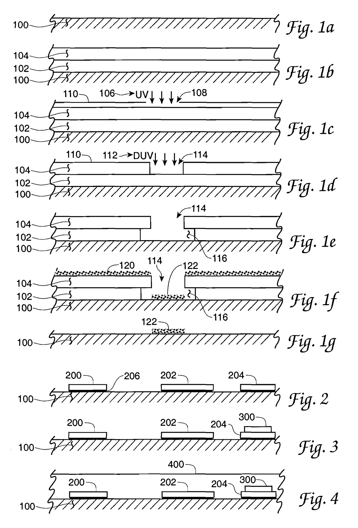
[0056]FIG. 1 in the drawings shows a sequence of steps usable to form a number of physical portions of a MEMS switch assembly and its electrical contacts in according with the present invention. In the FIG. 1 drawings a plurality of steps as appear in the views of FIG. 1A through FIG. 1F are employed in a sequence that is used multiple times in a switch and contact formation process. In a certain sense therefore the FIG. 1 sequence of steps may be likened to a subroutine in a computer program, a subroutine that is called into execution multiple times by a higher-level routine.

[0057]The FIG. 1 sequence commences with a substrate 100 that is composed of for example sapphire and that has been cleaned with a known buffered oxide etch, isopropyl alcohol and acetone sequence. The substrate 100 may have a thickness in the range of 500 nanometers, a surface roughness of 100 angstroms and may be supported on a vacuum chuck fixture during the FIG. 1 processing. This substrate 100 is covered w...


PUM


Abstract

A MEMS switch fabrication process and apparatus inclusive of a bulbous rounded surface movable contact assembly that is integral with the switch movable element and achieving of long contact wear life with low contact electrical resistance. The disclosed process is compatible with semiconductor integrated circuit fabrication materials and procedures and includes an unusual photoresist reflow step in which the bulbous contact shape is quickly defined in three dimensions from more easily achieved integrated circuit mask and etching-defined precursor shapes. A plurality of differing photoresist materials are used in the process. A large part of the contact and contact spring formation used in the invention is accomplished with low temperature processing including electroplating. Alternate processing steps achieving an alloy metal contact structure are included. Use of a subroutine of processing steps to achieve differing but related portions of the electrical contact structure is also included.

Description

CROSS REFERENCE TO RELATED PATENT DOCUMENTS[0001]This application is a division of application Ser. No. 11 / 047,345, filed Jan. 31, 2005, now U.S. Pat. No. 7,601,554, issued on Oct. 13, 2009. This application is somewhat related to commonly assigned patent application “RADIO FREQUENCY MEMS SWITCH CONTACT METAL SELECTION”, Ser. No. 11 / 047,344, filed Jan. 31, 2005, now U.S. Pat. No. 7,235,750, issued on Jan. 26, 2007. The contents of both related applications are hereby incorporated by reference.RIGHTS OF THE GOVERNMENT[0002]The invention described herein may be manufactured and used by or for the Government of the United States for all governmental purposes without the payment of any royalty.BACKGROUND OF THE INVENTION[0003]Radio frequency switches are used in many aspects of present day communication systems and radar systems including for example in cellular telephones and phased array radar antennas. Today, such radio frequency switching is often accomplished with the use of solid-...

Claims


Application Information

Patent Timeline
Patent Type & Authority Patents(United States)
IPC IPC(8): H01L29/78
CPCB81C1/00103B81C1/0015B81B2201/014B81B2203/0118B81B2203/019B81B2203/04H01H2001/0052
Inventor COUTU, JR., RONALD A.KLADITIS, PAUL E.CRANE, ROBERT L.
Owner THE UNITED STATES OF AMERICA AS REPRESETNED BY THE SEC OF THE AIR FORCE
Why Eureka
Try Eureka