
Expandable LED array interconnect

a technology of led arrays and interconnections, which is applied in the direction of discharge tubes luminescnet screens, semiconductor devices for light sources, lighting and heating apparatus, etc., can solve the problems of reducing the efficiency of the array, complex circuitry needed to connect the arrays, and difficulty in providing the necessary electrical connections to power the led arrays

Active Publication Date: 2011-03-01
CREELED INC
View PDF29 Cites 49 Cited by
  • Summary
  • Abstract
  • Description
  • Claims
  • Application Information

AI Technical Summary

Benefits of technology

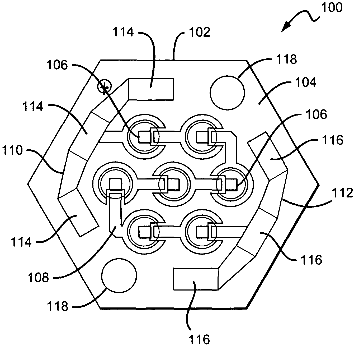
The present invention relates to a light emitting device that has a substrate with multiple edges and a top surface. The device has input and output terminals on the substrate edges. The device also has at least one lighting element connected between the input and output terminals. The invention also includes an LED array element that has a substrate with multiple edges and a top surface. The element has input and output terminals and at least one LED connected between the terminals. The invention also includes an expandable LED array with multiple LED array elements that have input and output terminals and a network of conductors for powering the elements. The technical effects of the invention include improved efficiency, flexibility, and durability of LED arrays.

Problems solved by technology

Providing the necessary electrical connections to power the LED arrays can be challenging.
As the number of LED arrays that are grouped together increases, the circuitry needed to connect the arrays can become complex and expensive.
The circuit topology required to power the arrays often requires circuit elements that cannot be mounted on the surface of the arrays.
This can result in circuit elements that obscure the light emitters and prevent the light from escaping to the outside environment, greatly decreasing the efficiency of the arrays.

Method used


Image

  • Expandable LED array interconnect
  • Expandable LED array interconnect
  • Expandable LED array interconnect

Examples


Embodiment Construction

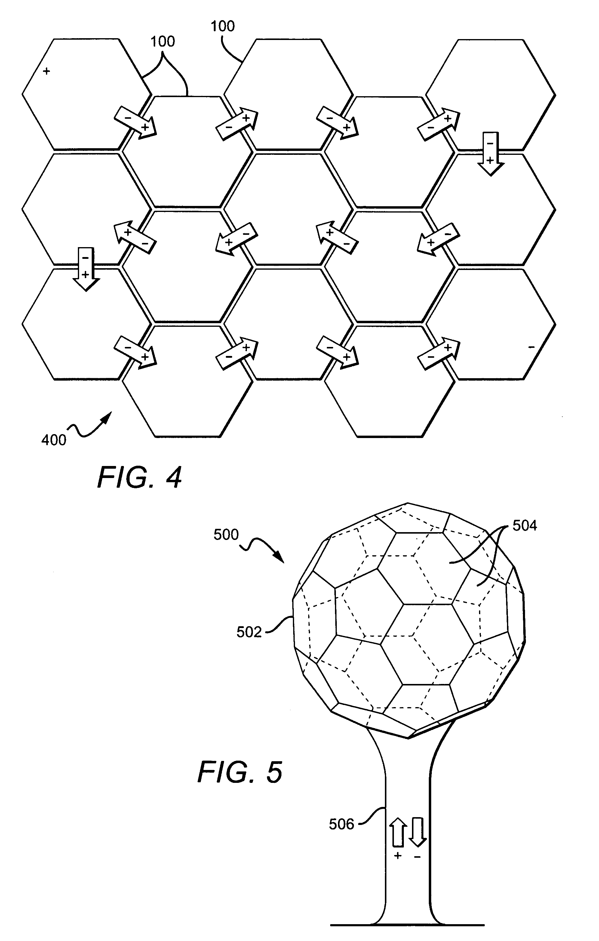
The present invention relates to light emitting devices, and in particular, light emitting devices that can be used as individual array elements that can be arranged in a pattern to increase luminescent output. The invention also relates to an expandable array of light emitting elements (e.g., LEDs). In one embodiment, at least one light emitter is disposed on a substrate and connected between input and output terminals located on opposite sides of the substrate. Multiple emitters may be disposed on the substrate in a pattern. These emitters may be connected between the input and output terminals serially, in parallel, or in a combination thereof. The input and output terminals are disposed on the top surface of the substrate along the edges such that they are accessible from a plurality of the edges. By increasing the ways in which the array elements can be interconnected, the arrangement of the contact pads provides improved flexibility when designing the layout for the light emit...


PUM


Abstract

A light emitting device that can function as an array element in an expandable array of such devices. The light emitting device comprises a substrate that has a top surface and a plurality of edges. Input and output terminals are mounted to the top surface of the substrate. Both terminals comprise a plurality of contact pads disposed proximate to the edges of the substrate, allowing for easy access to both terminals from multiple edges of the substrate. A lighting element is mounted to the top surface of the substrate. The lighting element is connected between the input and output terminals. The contact pads provide multiple access points to the terminals which allow for greater flexibility in design when the devices are used as array elements in an expandable array.

Description

BACKGROUND OF THE INVENTION1. Field of the InventionThe invention relates to lighting systems, and more particularly to interconnected light emitting diode (LED) arrays.2. Description of the Related ArtLEDs are semiconductor photon sources that can serve as highly efficient electronic-to-photonic transducers. They are typically forward-biased p-n junctions fabricated from a semiconductor material that emit light via injection electroluminescence. Their small size, high efficiency, high reliability, and compatibility with electronic systems make them very useful for a multitude of applications. Recent advancements have yielded high-power LEDs in a range of colors. This new generation of LEDs is useful in applications requiring a higher intensity light output such as high-power flash lights, airplane lighting systems, fiber-optic communication systems, and optical data storage systems.High-flux lighting solutions are required by various modern applications such as street lighting, air...

Claims


Application Information

Patent Timeline
Patent Type & Authority Patents(United States)
IPC IPC(8): H01L33/00H01L33/48
CPCF21K9/00F21S2/005H01L25/0753F21Y2101/02F21Y2105/001F21Y2111/007F21Y2101/025H01L2924/0002F21Y2105/10F21Y2115/30F21Y2115/10F21Y2107/40H01L2924/00
Inventor YUAN, THOMAS CHENG-HSINKELLER, BERND
Owner CREELED INC
Learn More