
Method for manufacturing an electrical test probe

a technology of test probes and manufacturing methods, applied in the field of electric test probes, can solve the problems of microscopic test probes, achieve the effects of reducing the stress acting on the base portion, and improving the durability of test probes

Active Publication Date: 2010-06-15
NIHON MICRONICS
View PDF2 Cites 6 Cited by
  • Summary
  • Abstract
  • Description
  • Claims
  • Application Information

AI Technical Summary

Benefits of technology

This design enhances the durability of the probe tip section by reducing stress on the base portion, improving mechanical strength and extending the probe's lifespan without increasing overall thickness or weight, thus maintaining reliability during testing.

Problems solved by technology

Meanwhile, such a probe is microscopic.

Method used


Image

  • Method for manufacturing an electrical test probe
  • Method for manufacturing an electrical test probe
  • Method for manufacturing an electrical test probe

Examples


Embodiment Construction

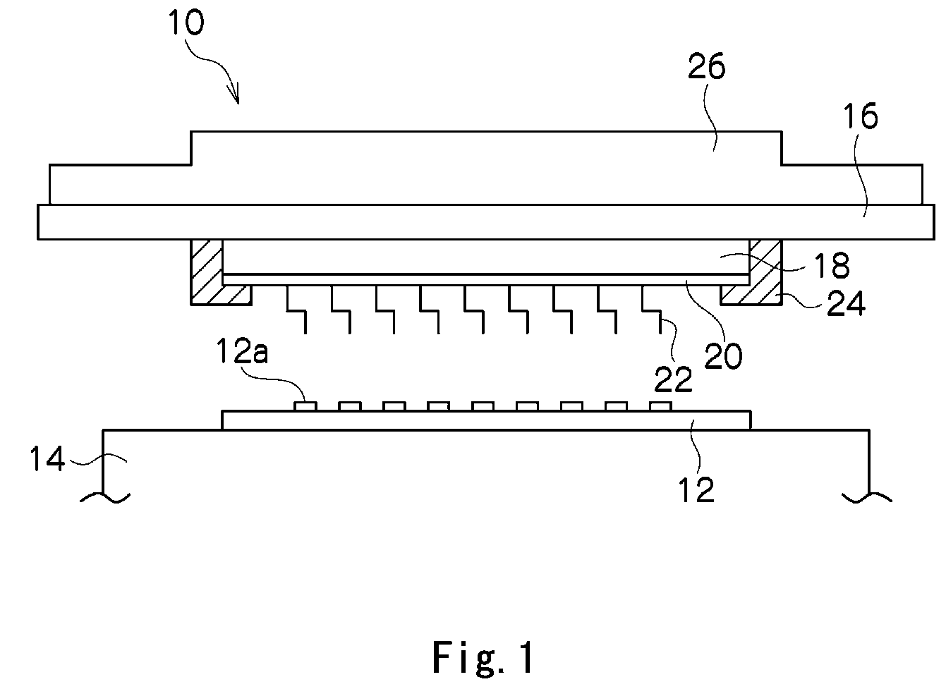
[0033]A probe assembly 10 according to the present invention is used for an electrical test of a plurality of integrated circuits (not shown) formed on a semiconductor wafer 12 as shown in FIG. 1. The semiconductor wafer 12 is removably held on a vacuum chuck 14, for example, with a plurality of electrodes 12a formed on its one surface directing upward. The probe assembly 10 is supported by a not shown frame member to be movable relatively to the vacuum chuck 14 in directions approaching and distanced from the semiconductor wafer 12 on the vacuum chuck 14 for the electrical test of the aforementioned integrated circuits of the semiconductor wafer 12.

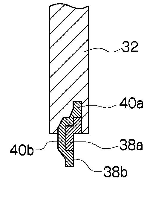
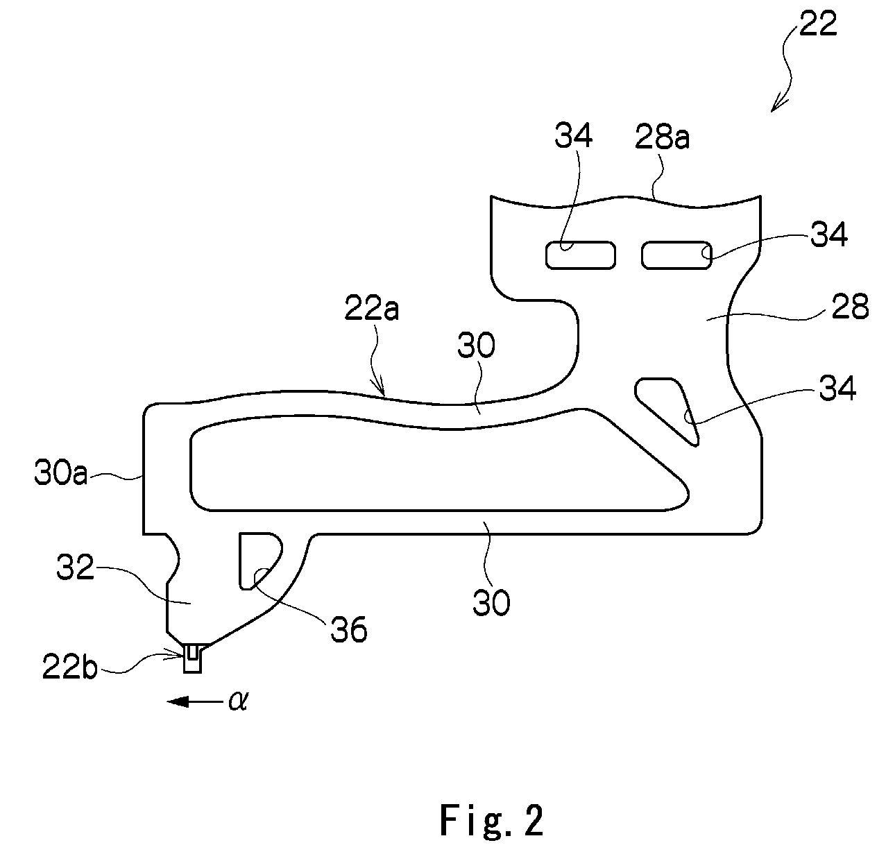
[0034]The probe assembly 10 comprises a printed wiring board 16 and a probe board 20 piled up on the printed wiring board via a ceramic board 18. On one surface of the probe board 20 are arranged and attached a plurality of probes 22 according to the present invention. The ceramic board 18 and the probe board 20 are attached to the print...


PUM

PropertyMeasurementUnit
thicknessaaaaaaaaaa
shapeaaaaaaaaaa
toughnessaaaaaaaaaa

Abstract

A probe tip section of an electrical test probe has a laminated structure consisting of a first deposition portion and a second deposition portion covering the first deposition portion, and by the laminated structure, a maximum cross-sectional area portion at which the cross-sectional area of the probe tip section is increased to a base portion is provided between a tip end of the probe tip section and the base portion in the probe tip section. At the maximum cross-sectional area portion, a dimension in the X direction as seen on a flat surface perpendicular to a protruding direction of the probe tip section is increased in a one-dimensional way, and in addition, a dimension in the Y direction perpendicular to the X direction is increased from the tip end toward the base portion, as a result of which the cross-sectional area of the probe tip section can be increased in a two-dimensional way. Thus, the cross-sectional area at the maximum cross-sectional area portion reaching the base portion of the probe tip section can be made to be larger than in the conventional case, and along with the increase of the cross-sectional area, the stress acting on the base portion can be lowered.

Description

BACKGROUND OF THE INVENTION[0001]The present invention relates to an electrical test probe suitable for use in an electrical test of a plurality of semiconductor integrated circuits formed on a semiconductor wafer and a method for manufacturing the same.[0002]A plurality of semiconductor integrated circuits formed on a semiconductor wafer generally undergo an electrical test before being separated into respective chips to determine whether or not they are manufactured in accordance with the specification. In this electrical test, a probe assembly comprising electrical test probes to be connected to electrodes of devices under test that are the respective semiconductor integrated circuits is used. The devices under test are connected to a tester via this probe assembly.[0003]One of the conventional probes used for this probe assembly is one comprising a plate-shaped probe main body section and a probe tip section provided on the probe main body section and that is to abut on an elect...

Claims


Application Information

Patent Timeline
Patent Type & Authority Patents(United States)
IPC IPC(8): B05D5/12
CPCG01R1/06733G01R1/06755Y10T29/49204Y10T29/49117
Inventor HIRAKAWA, HIDEKIYAMADA, YUKOYOSHIZAWA, YOSUKEHAYASHIZAKI, TAKAYUKISOMA, AKIRAKUNIYOSHI, SHINJI
Owner NIHON MICRONICS
Learn More