Edge illuminated photodiodes
a photodiode and edge illumination technology, applied in the field of photodiodes, can solve the problems of low responsivity due to edge surface recombination, the difficulty of controlling quantum efficiency, and the current photodiode, so as to improve the operational and structural characteristics
- Summary
- Abstract
- Description
- Claims
- Application Information
AI Technical Summary
Benefits of technology
Problems solved by technology
Method used
Image
Examples
first embodiment
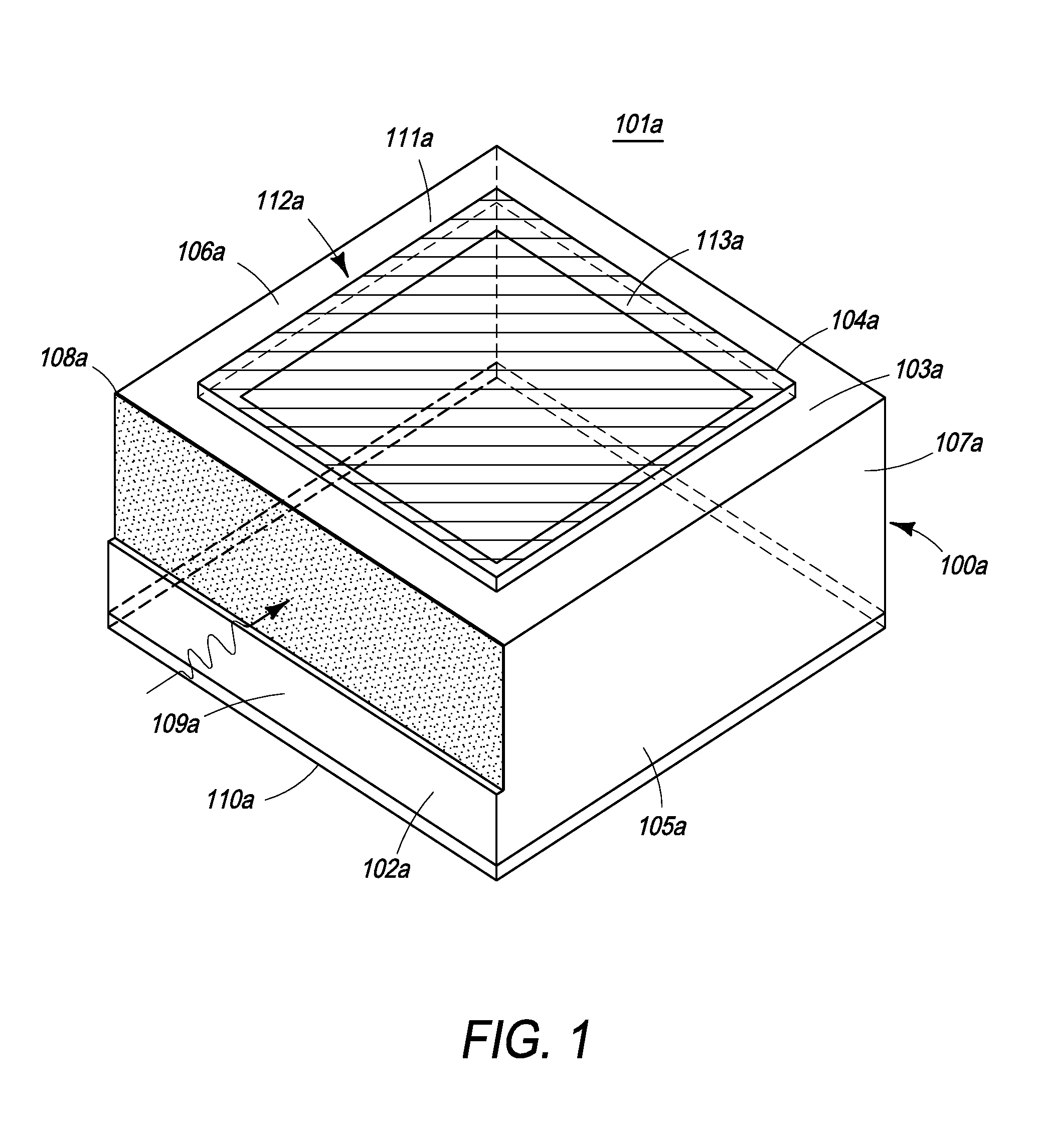
[0027]In a first embodiment, the edge illuminated photodiode is incorporated in a photochip having six distinct facets, namely proximate, distant, top, bottom, left, and right respectively. The proximate and distant facets are substantially parallel to each other. The top and bottom facets are substantially parallel to each other, and the left and right facets are substantially parallel to each other. The proximate facet substantially comprises an n+ diffused region. The bottom facet comprises a cathode metallization layer. The top facet comprises two regions, namely an anode metallization region and a p+ doped region. The p+ doped region is juxtaposed to the anode metallization region.
second embodiment
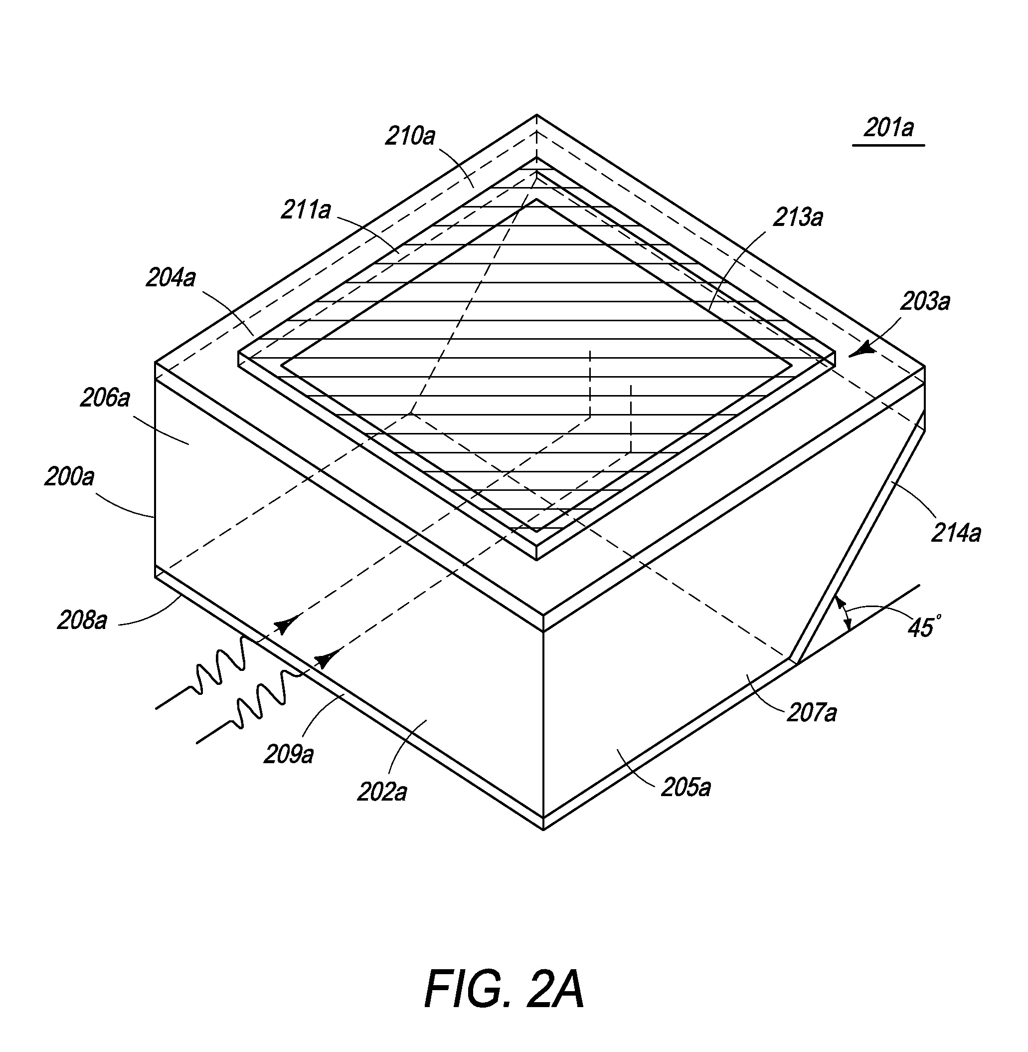
[0028]In second embodiment, an edge illuminated photodiode is incorporated in a substrate having seven distinct facets. Six facets include a proximate, distant, top, bottom, left, and right facet, respectively. The proximate and distant facets are substantially parallel to each other. The top and bottom facets are substantially parallel to each other, and the left and right facets are substantially parallel to each other. The seventh facet is formed at an angle to no less than two facets, i.e., the distant and bottom facets, respectively. Preferably the angle of formation, measured relative to the internal face of each facet (the sides facing the inside of the photodiode), is greater than 90 degrees. More preferably, the angle of formation is 135 degrees.
[0029]In one embodiment, the top facet comprises two regions, namely an anode metallization region and a p+ doped and textured region. The p+ region, juxtaposed to the anode metallization region, is textured to reduce reflectance at...
third embodiment
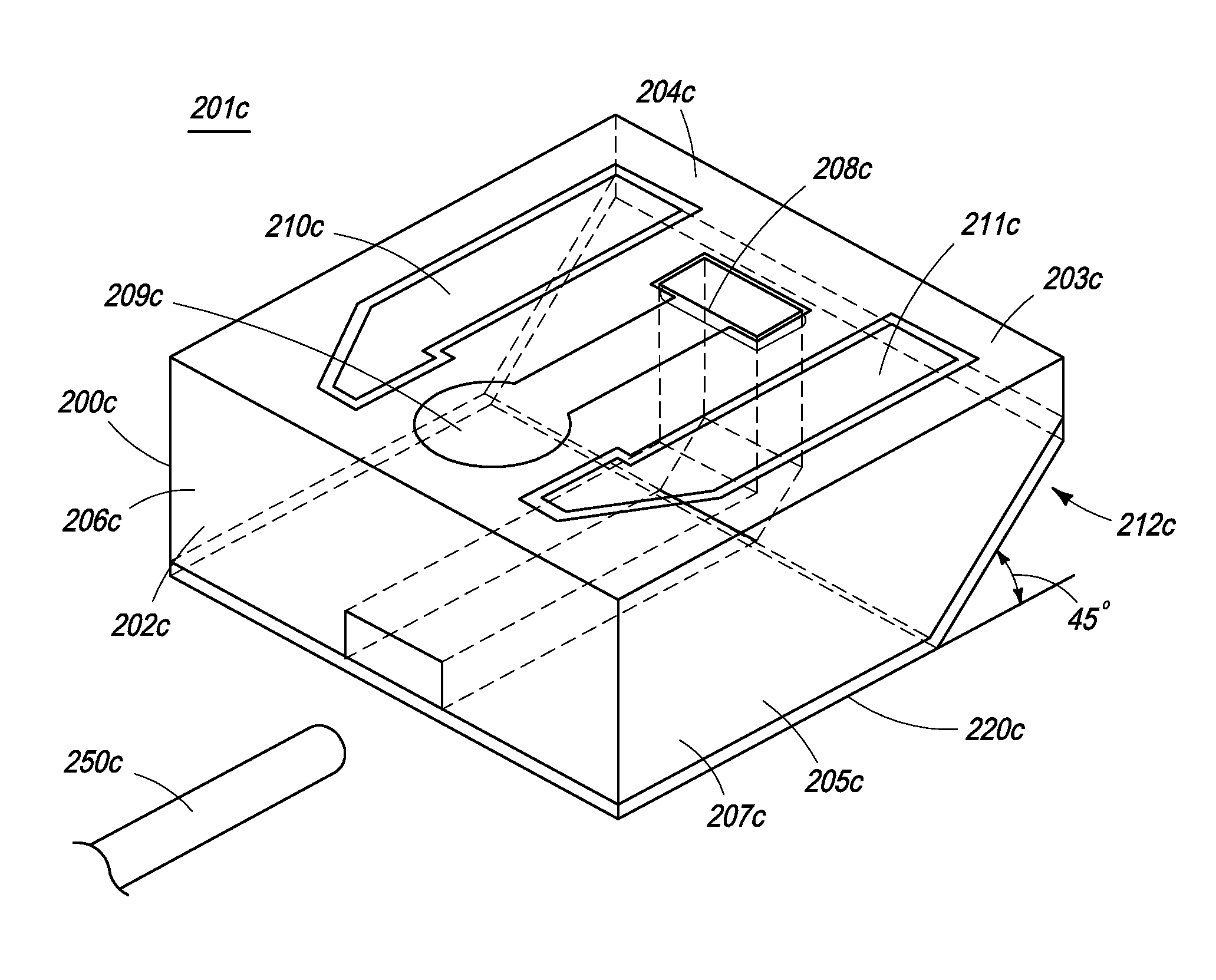
[0049]an edge illuminated photodiode of the present invention is depicted in FIG. 2c. Photodiode 201c comprises photochip 200c, which is made of a suitable semiconductor material possessing apt geometrical specifications. For example, and by no way of limitation, photochip 200c comprises silicon that is cuboidal in geometry. The cuboid (or rectangular parallelepiped) shaped photochip 200c has six distinct facets. For purposes of elucidation, the sides or facets of photochip 200c have been enumerated as proximate 202c, distant 203c, top 204c, bottom 205c, left 206c, and right 207c. Persons of ordinary skill would appreciate that the present designation of photochip geometry is not limited to the description provided herein and can be adjusted to suit other design, fabrication, and functional specifications.
[0050]Bottom surface 205a is subjected to metallization in accordance with the principles of the present invention. Consequently, bottom facet 205a comprises a finish layer 220c. F...
PUM
 Abstract
Description
Claims
Application Information
 - R&D
- Intellectual Property
- Life Sciences
- Materials
- Tech Scout
- Unparalleled Data Quality
- Higher Quality Content
- 60% Fewer Hallucinations
Browse by: Latest US Patents, China's latest patents, Technical Efficacy Thesaurus, Application Domain, Technology Topic, Popular Technical Reports.
© 2025 PatSnap. All rights reserved.Legal|Privacy policy|Modern Slavery Act Transparency Statement|Sitemap|About US| Contact US: help@patsnap.com


