Buried asymmetric junction ESD protection device
a protection device and asymmetric junction technology, applied in the direction of semiconductor devices, semiconductor/solid-state device details, electrical apparatus, etc., can solve the problems of increasing the overall manufacturing cost, reducing the overall manufacturing yield, and difficult or impossible to achiev
- Summary
- Abstract
- Description
- Claims
- Application Information
AI Technical Summary
Benefits of technology
Problems solved by technology
Method used
Image
Examples
first embodiment
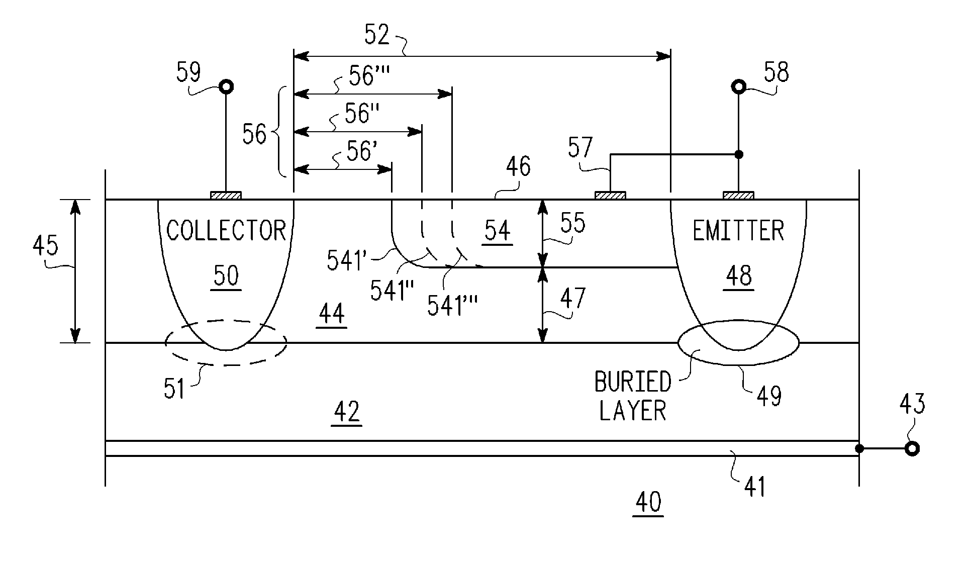
[0020] there is provided a lateral electrostatic discharge (ESD) protection device (40), comprising, a semiconductor substrate (42) of a first conductivity type and first doping level, a semiconductor layer (44) overlying the substrate (42), and of the first conductivity type and a second doping level and having an outer surface (46) spaced a first distance (45) from the substrate (42), emitter (48) and collector (50) regions of a second, opposite, conductivity type, laterally spaced apart by a second distance (52), and having third doping level greater than the second doping level, a well region (54) of the first conductivity type in but not extending through the semiconductor layer (44) and having a doping level higher than the second doping level but less than or equal to the third doping level, and extending laterally from the emitter region (48) toward but separated from the collector region (50) by a third distance (56), and a buried layer (49) of the second conductivity type ...
second embodiment
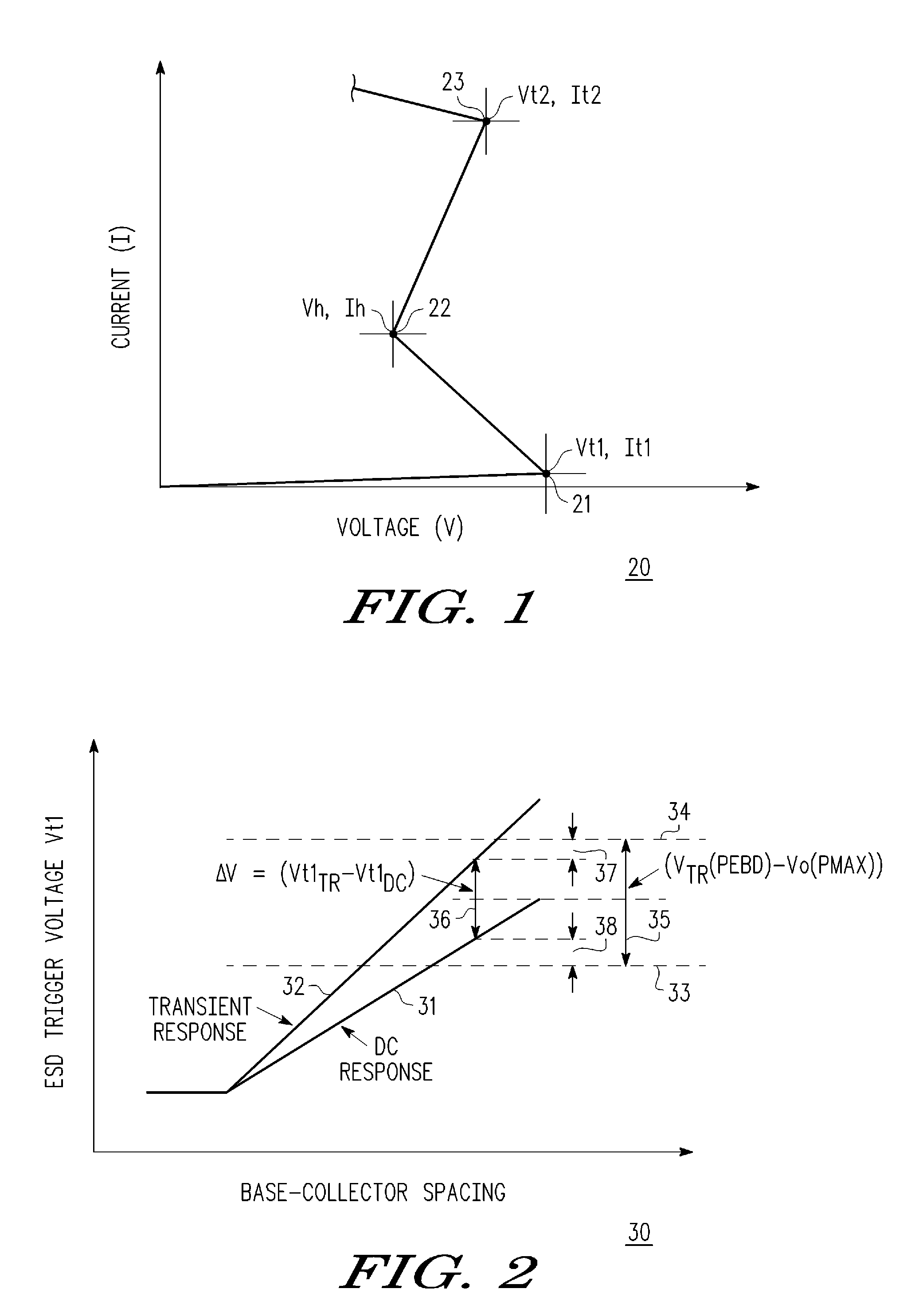
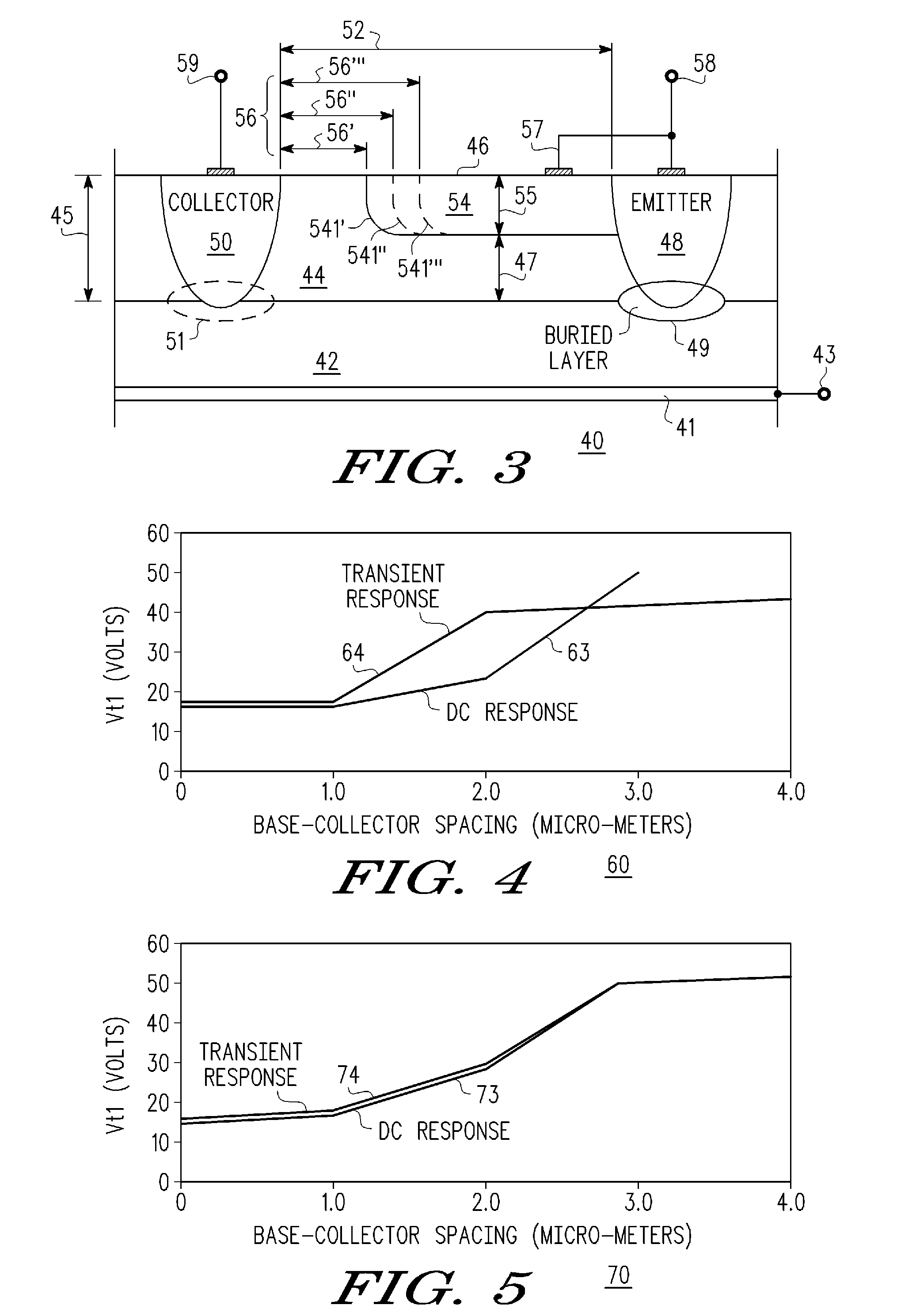
[0021] there is provided a lateral bipolar electrostatic discharge (ESD) protection device (40) having a trigger voltage Vt1, comprising, a semiconductor (SC) substrate (42), an overlying epitaxial SC layer (44), emitter-collector regions (48, 50) in the SC layer (44), laterally spaced apart by a first distance (52), a base region (54) adjacent the emitter region (48) in the epitaxial SC layer (44) extending laterally toward and separated from the collector region (50) by a base-collector spacing (56) in the epitaxial layer (44), which base-collector spacing (56) is chosen to set a predetermined ESD trigger voltage Vt1, and a buried layer region (49) under the emitter region (48) Ohmically coupled thereto, but without a comparable buried layer region (51) under the collector region (50), thereby providing an asymmetrical structure whose DC trigger voltage (Vt1DC) and transient trigger voltage (Vt1TR) are approximately equal. According to a further embodiment, the buried layer region...
third embodiment
[0022] there is provided a lateral electrostatic discharge (ESD) protection device (40), comprising, a semiconductor substrate (42) of a first conductivity type and first doping level, a semiconductor layer (44) overlying the substrate (42), and of the first conductivity type and a second doping level equal or less than the first doping level and having an outer surface (46) spaced a first distance (45) from the substrate (42), emitter (48) and collector (50) regions of a second, opposite, conductivity type, laterally spaced apart by a second distance (52), and having third doping levels greater than the second doping level, a well region (54) of the first conductivity type in but not extending through the semiconductor layer (44) and having a doping level higher than the second doping level and extending laterally from the emitter region (48) toward but separated from the collector region (50) by a third distance (56), wherein the third distance (56) is in the range of about 0 to 3...
PUM
 Abstract
Description
Claims
Application Information
 - R&D
- Intellectual Property
- Life Sciences
- Materials
- Tech Scout
- Unparalleled Data Quality
- Higher Quality Content
- 60% Fewer Hallucinations
Browse by: Latest US Patents, China's latest patents, Technical Efficacy Thesaurus, Application Domain, Technology Topic, Popular Technical Reports.
© 2025 PatSnap. All rights reserved.Legal|Privacy policy|Modern Slavery Act Transparency Statement|Sitemap|About US| Contact US: help@patsnap.com


