Stacked electronic component package having film-on-wire spacer
- Summary
- Abstract
- Description
- Claims
- Application Information
AI Technical Summary
Benefits of technology
Problems solved by technology
Method used
Image
Examples
Embodiment Construction
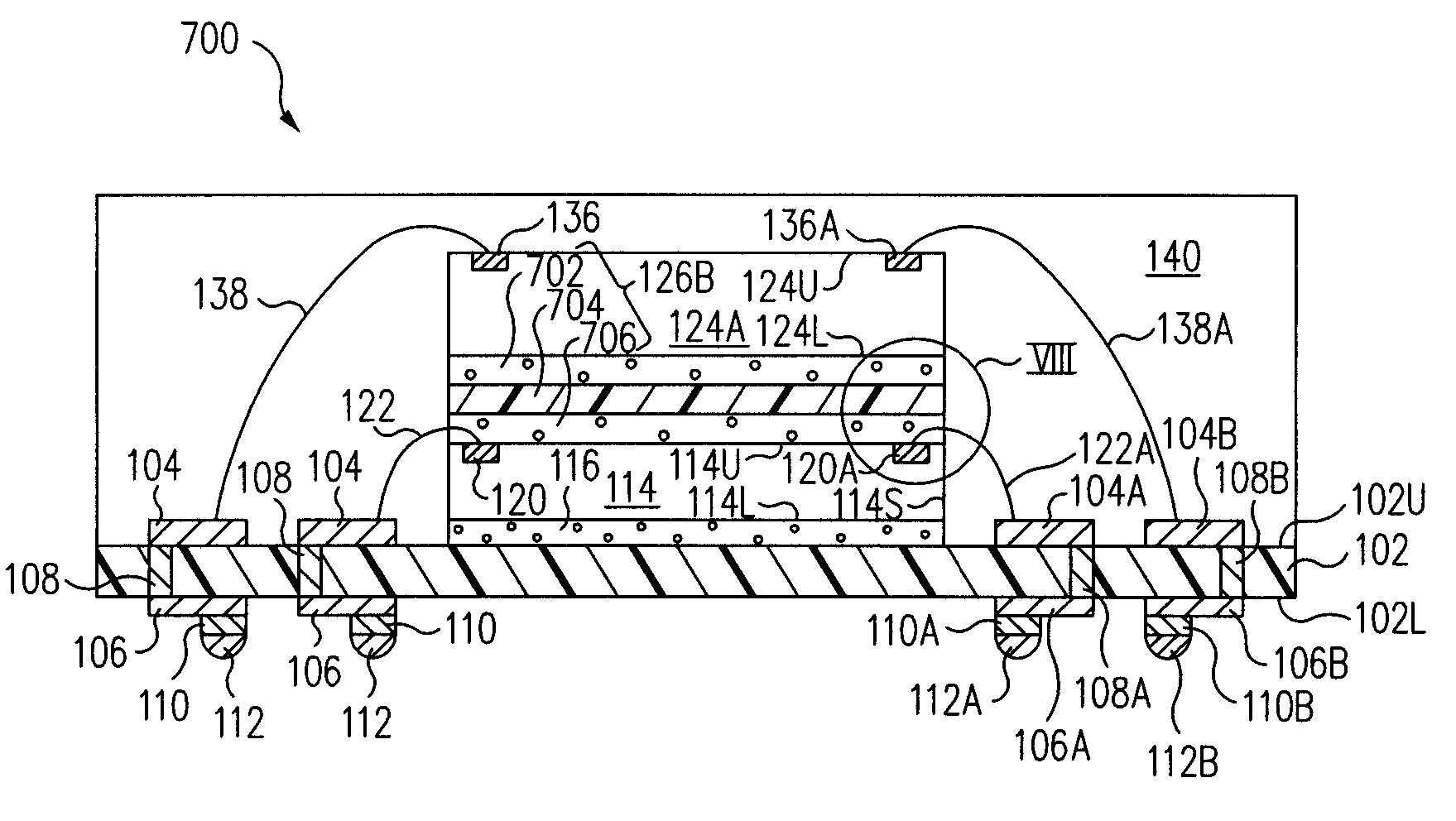
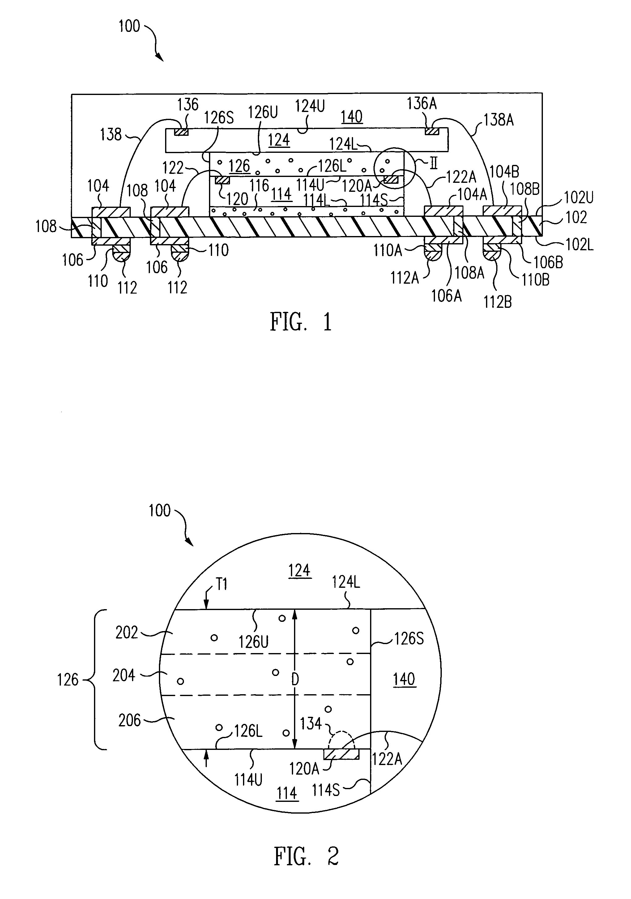
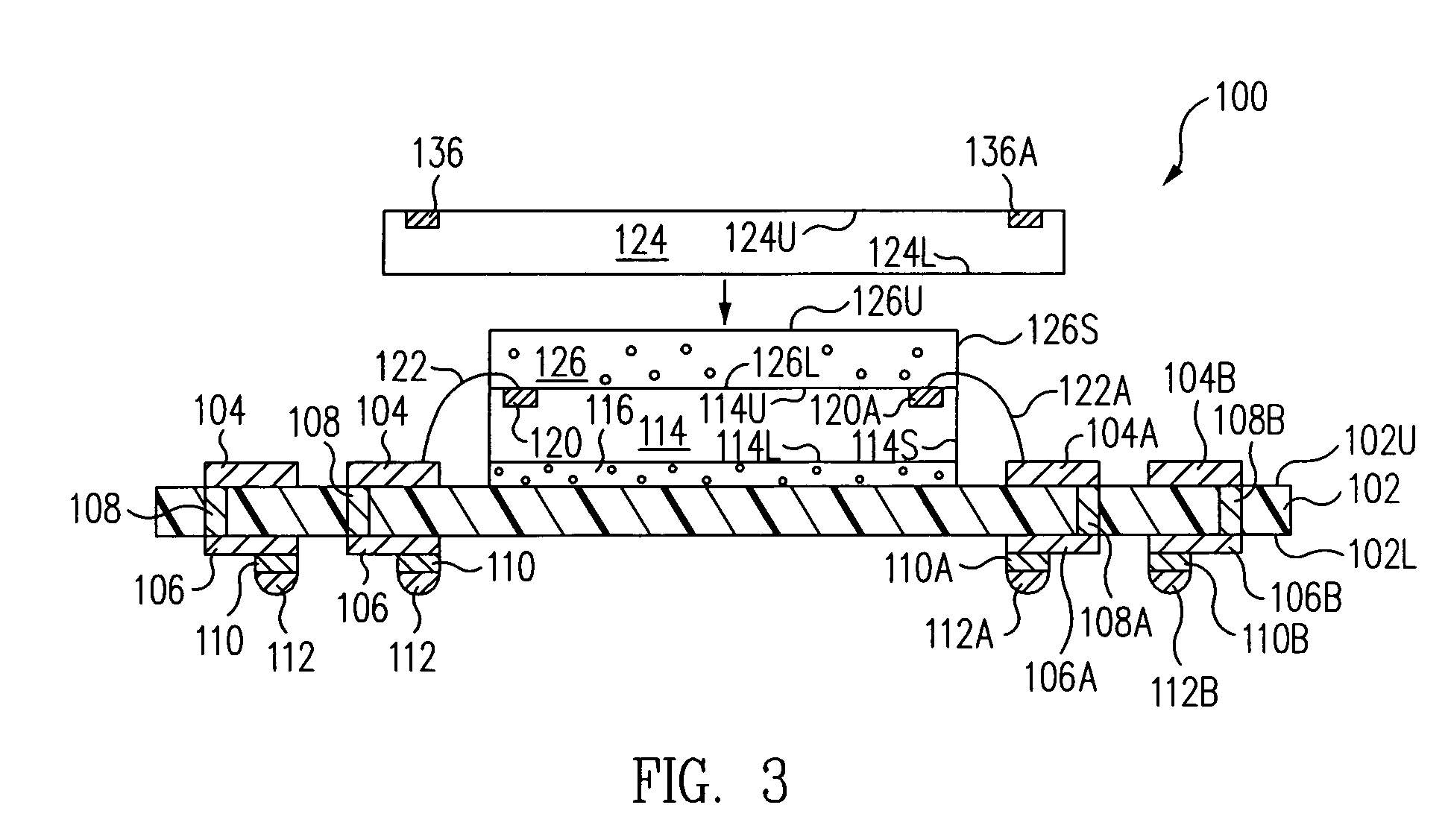
[0030]In accordance with one embodiment, referring to FIGS. 1 and 2 together, a film-on-wire spacer 126 covers an entire upper surface 114U of a lower electronic component 114. Accordingly, an upper electronic component 124 is supported above bond pads 120 and lower bond wires 122 of lower electronic component 114. This decreases the stress on upper electronic component 124, e.g., during wirebonding, and thus decreases the chance of cracking upper electronic component 124. Further, lower bond wires 122 are enclosed in and protected by film-on-wire spacer 126. Further, film-on-wire spacer 126 is thin resulting in a minimum height of stacked electronic component package 100.
[0031]More particularly, FIG. 1 is a cross-sectional view of a stacked electronic component package 100 in accordance with one embodiment of the present invention. Stacked electronic component package 100 includes a substrate 102, e.g., formed of metal, with ceramic, pre-molded plastic or laminate materials, althou...
PUM
 Abstract
Description
Claims
Application Information
 - R&D
- Intellectual Property
- Life Sciences
- Materials
- Tech Scout
- Unparalleled Data Quality
- Higher Quality Content
- 60% Fewer Hallucinations
Browse by: Latest US Patents, China's latest patents, Technical Efficacy Thesaurus, Application Domain, Technology Topic, Popular Technical Reports.
© 2025 PatSnap. All rights reserved.Legal|Privacy policy|Modern Slavery Act Transparency Statement|Sitemap|About US| Contact US: help@patsnap.com


