
Circuit to compensate threshold voltage variation due to process variation

a threshold voltage and process variation technology, applied in the field can solve the problems of increasing the time required to design semiconductor integrated circuits, affecting the performance of semiconductor integrated circuits thus designed, and essentially not being able to avoid

Inactive Publication Date: 2010-02-23
INT BUSINESS MASCH CORP
View PDF11 Cites 9 Cited by
  • Summary
  • Abstract
  • Description
  • Claims
  • Application Information

AI Technical Summary

Problems solved by technology

However, since it is difficult to presume device performance variations, the period of time required to design semiconductor integrated circuits is increased, and it is necessary to give timing margins to allow semiconductor integrated circuits to operate in worst cases.
The semiconductor integrated circuits thus designed tend to suffer performance reductions.
As the device manufacturing variations are the result of physical configuration variations and chemical compositions of the semiconductor devices, these variations essentially cannot be avoided because manufacturing errors cannot fully be eliminated.
While threshold voltage (Vt) must be matched across the chip, long-range Vt mismatches are known to exist due to long-range intra-die process variation from RTA.
As these long range mismatch solutions are generally required to act on a very large area, these solutions have been found to be prohibitively expensive.

Method used


Image

  • Circuit to compensate threshold voltage variation due to process variation
  • Circuit to compensate threshold voltage variation due to process variation
  • Circuit to compensate threshold voltage variation due to process variation

Examples


Embodiment Construction

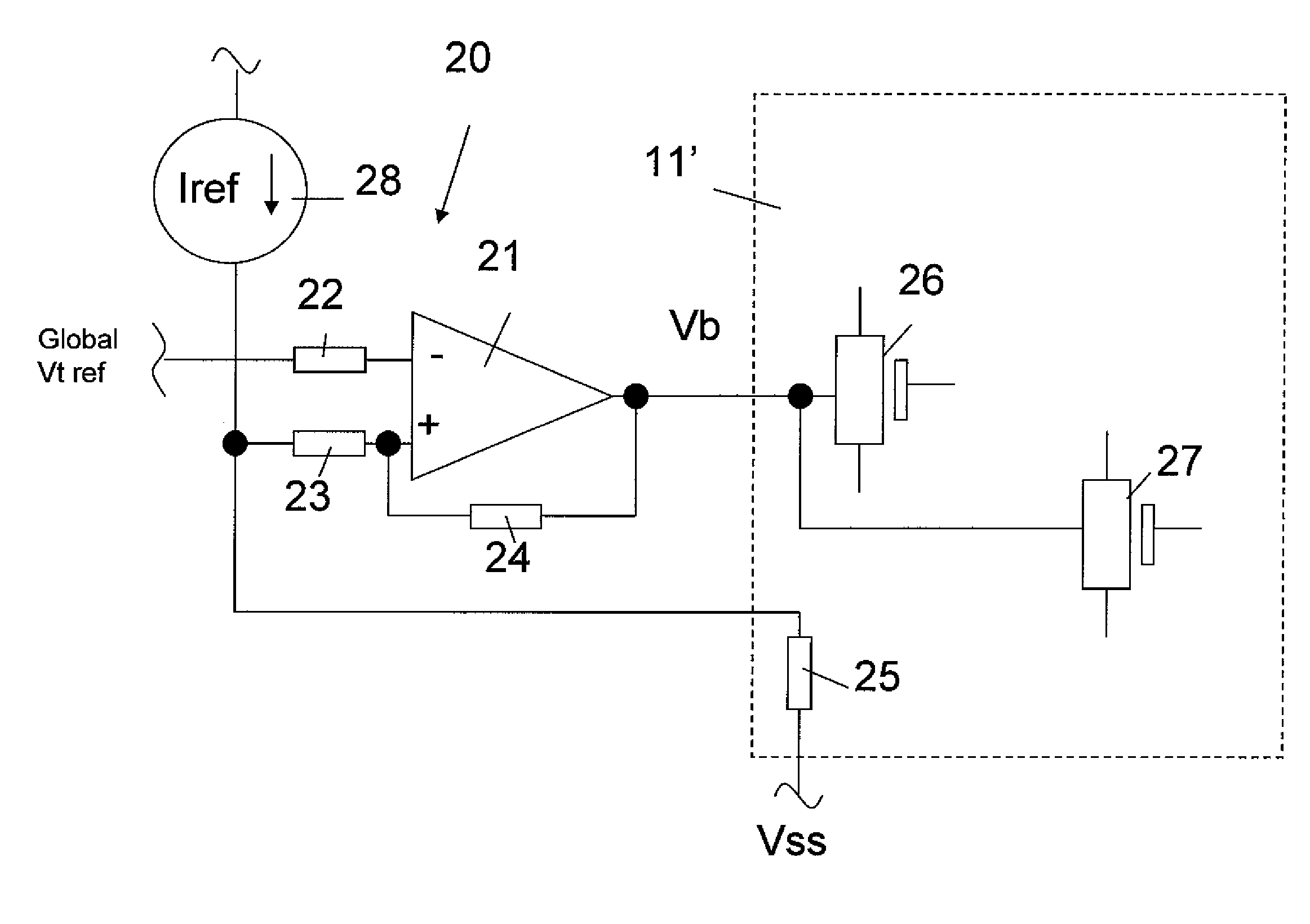
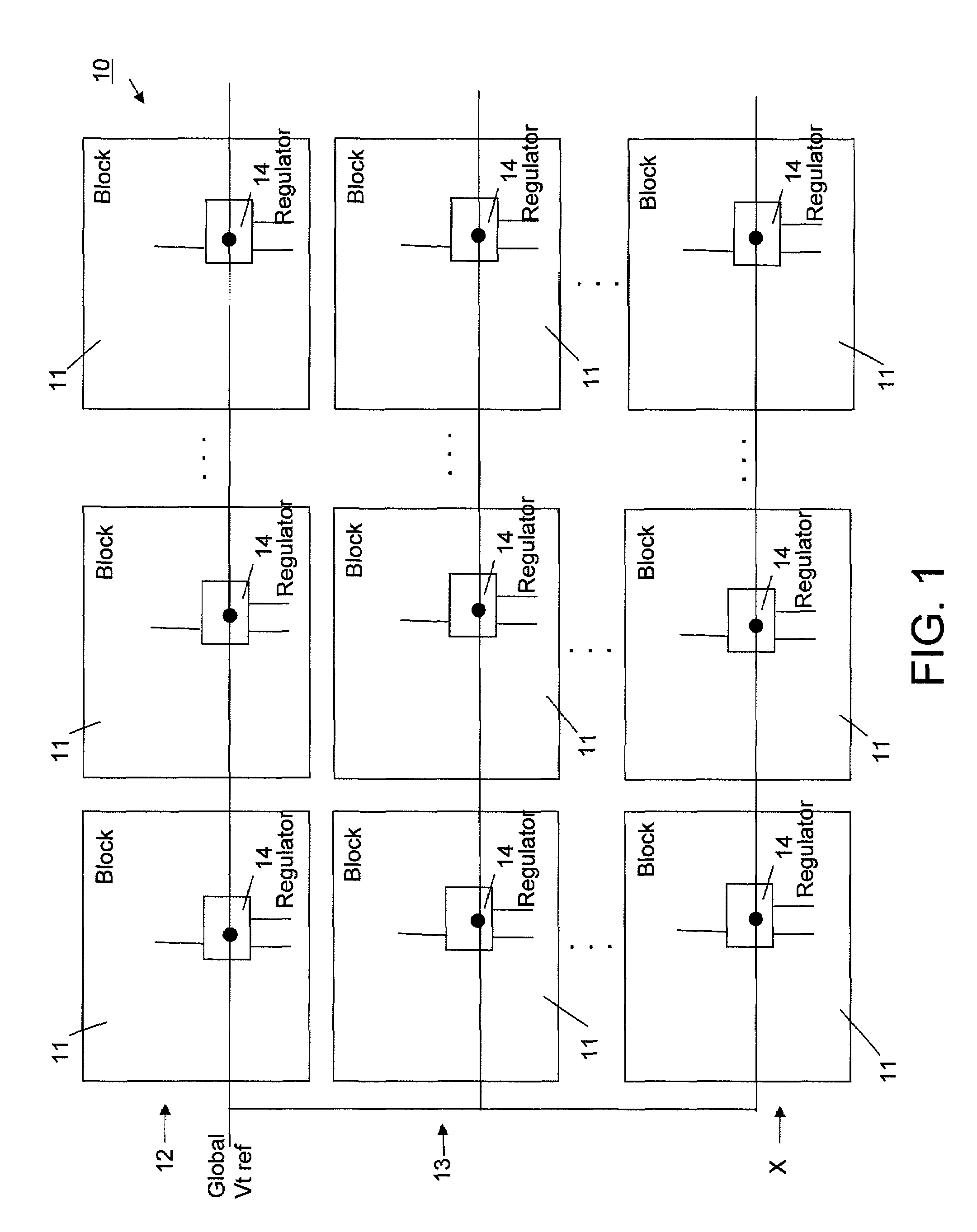
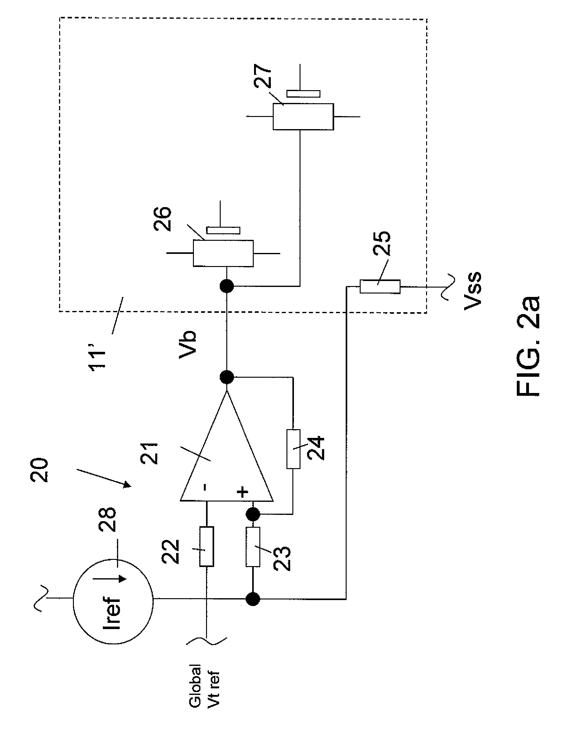
[0013]The present invention is directed to a circuit structured and arranged to sample the local process environment and adjust body bias to keep the threshold voltage matched to a “master transistor” within the die, which enables accurate operation of circuits requiring precise Vt matching, e.g., current mirrors. According to an embodiment of the invention, a well grid is broken up into blocks that are a fraction, e.g., one-half the size (such as linear size), of an expected RTA length scale, and at least one voltage regulator is coupled to each block. According to a further embodiment of the invention, the block dimensions can be, e.g., 2 mm×2 mm for spike RTA.

[0014]As illustrated in FIG. 1, an integrated circuit chip 10 is shown in which system global variations in threshold voltage Vt of transistors are slowly varying over distance, e.g., due to long-range intra-die process variations in forming chip 10, e.g., from RTA. Thus, variations in threshold have a length scale, such tha...


PUM


Abstract

Structure and process for compensating threshold voltage variation due to process variation. The structure includes a circuit segmented into sub-blocks having a predetermined size corresponding to a characteristic length associated with a process variation. A local circuit is located in each circuit sub-block, and a reference signal coupled to each local circuit. The local circuit generates a compensation signal in response to the reference signal to adjust an electrical parameter of the respective sub-block to a predetermined value.

Description

FIELD OF THE INVENTION[0001]The present invention relates to a semiconductor integrated circuit and a process to compensate for device process variations of the semiconductor integrated circuit, i.e., variations of threshold voltages (Vt) of FETs.BACKGROUND DESCRIPTION[0002]Semiconductor integrated circuits are normally designed in view of process variations in forming the circuits. Specifically, process variations are presumed, and semiconductor integrated circuits are designed such that they will operate reliably for desired performance within the presumed range of process variation. However, since it is difficult to presume device performance variations, the period of time required to design semiconductor integrated circuits is increased, and it is necessary to give timing margins to allow semiconductor integrated circuits to operate in worst cases. The semiconductor integrated circuits thus designed tend to suffer performance reductions. There have recently been proposed variati...

Claims


Application Information

Patent Timeline
Patent Type & Authority Patents(United States)
IPC IPC(8): H03K3/01
CPCG05F3/205
Inventor CLARK, JR., WILLIAM F.NOWAK, EDWARD J.
Owner INT BUSINESS MASCH CORP
Learn More