Non-volatile memory device and fabricating method thereof

a memory device and non-volatile technology, applied in the direction of semiconductor devices, electrical devices, transistors, etc., can solve the problems of production cost increase, inability to meet economic efficiency, etc., and achieve the effects of avoiding the loss of charges, high energy gap, and effective storag

Inactive Publication Date: 2010-02-16
IND TECH RES INST
View PDF10 Cites 5 Cited by
  • Summary
  • Abstract
  • Description
  • Claims
  • Application Information

AI Technical Summary

Benefits of technology

[0011]Herein, the substrate may be a silicon substrate, or the material may be poly Si, Ni, Pt, TiN, Al, tantalum nitride, silicide or compounds thereof, etc. The material of the tunneling dielectric layer and the block dielectric layer is an oxide, for example, SiO2 or Al2O3 and etc.; or a high dielectric constant material with high energy gap, so as to simplify the process complexity.
[0012]Therein, the composite charge trapping layer contains many materials, which may be SiO2, Si3N4, Al2O3, HfO2, TiO2, Ta2O5, BaSrTiO3, PbLaZrTiO3, Y2O3, La2O3, a-Si, a-SiC, a-SiGe, a-Ge or combination thereof in any proportion. In fact, the composite charge trapping layer may be form by deposition process. For example, in the deposition of a tunneling dielectric layer, composite charge trapping layer and block dielectric layer with a chemical vapor deposition technique, an ingredient of a depositing material or the depositing material is adjusted to form a grading energy level structure, such that carriers are trapped or erased more easily in accordance with a variation in grading energy level. Therefore, the electrons are stored more effectively and the probability that the electric leakage occurs is reduced substantially. Otherwise, after the composite charge trapping layer is formed, an annealing process may be carried on, and many crystalline particles will be formed in the composite charge trapping layer after a suitable heat treatment, and thereby the charge storage capability of the device is further enhanced.
[0014]To achieve the above object, another non-volatile memory device is disclosed, which includes a substrate, a tunneling dielectric layer, a composite charge trapping layer, a block dielectric layer and a conductor layer, wherein the tunneling dielectric layer, the composite charge trapping layer, the block dielectric layer and the conductor layer are formed on the substrate sequentially. And, the composite charge trapping layer has a composition grading energy band structure. That is to say, the energy band structure of this composite charge trapping layer decreases first and then increases to form a quantum-well-like structure, such that the charges are stored more effectively to avoid the loss of charges. And the quantity of charges may also be adjusted freely by using energy level fluctuant structure and variation, thereby adjusting the shift value of the device threshold voltage.
[0015]Herein, the substrate may be a silicon substrate, or the material may be poly Si, Ni, Pt, TiN, Al, tantalum nitride, silicide or compounds thereof, etc. The material of the tunneling dielectric layer and the block dielectric layer is an oxide, for example SiO2 or Al2O3 and etc.; or a high dielectric constant material with high energy gap, thereby simplifying the process complexity.
[0017]Also, a plurality of crystalline particles is included in the composite charge trapping layer, and therefore the charge storage capability of the device is further enhanced. And the material of the composite charge trapping layer except the crystalline particle region is an amorphous material.

Problems solved by technology

However, the floating gate device can only store one bit, causing the production cost raised, so it cannot meet the economic efficiency.

Method used


Image

  • Non-volatile memory device and fabricating method thereof
  • Non-volatile memory device and fabricating method thereof
  • Non-volatile memory device and fabricating method thereof

Examples


Embodiment Construction

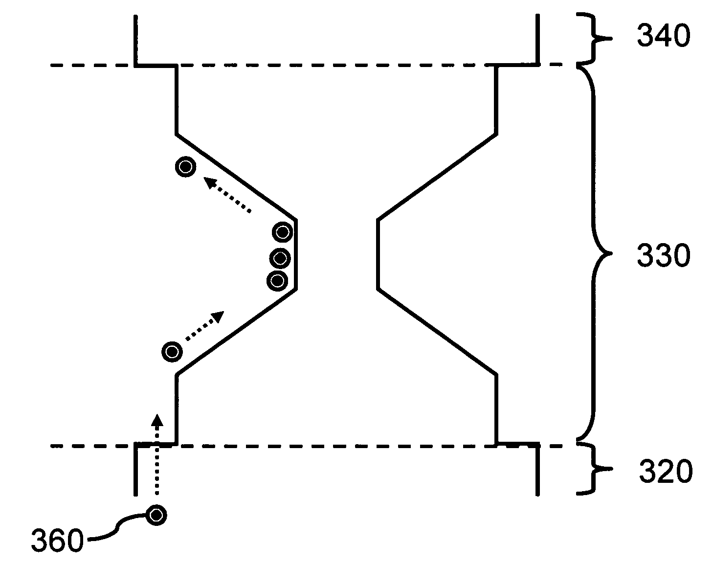
[0029]First, the object of the present invention is to replace the charge trapping device by a high dielectric constant or amorphous material having a grading energy level structure to form a charge trapping device with quantum-well-like structure. The variation in grading energy level of the material in the charge trapping device can be used to store charges more effectively, so as to avoid a loss of charge. And the quantity of the charge may also be adjusted freely by using energy level fluctuant structure and variation, thereby adjusting the shift value of the device threshold voltage.

[0030]Hereinafter, embodiments are illustrated to describe the content of the present invention in detail, in accompanying with the drawings. The symbols referred in the description are symbols of the reference drawings.

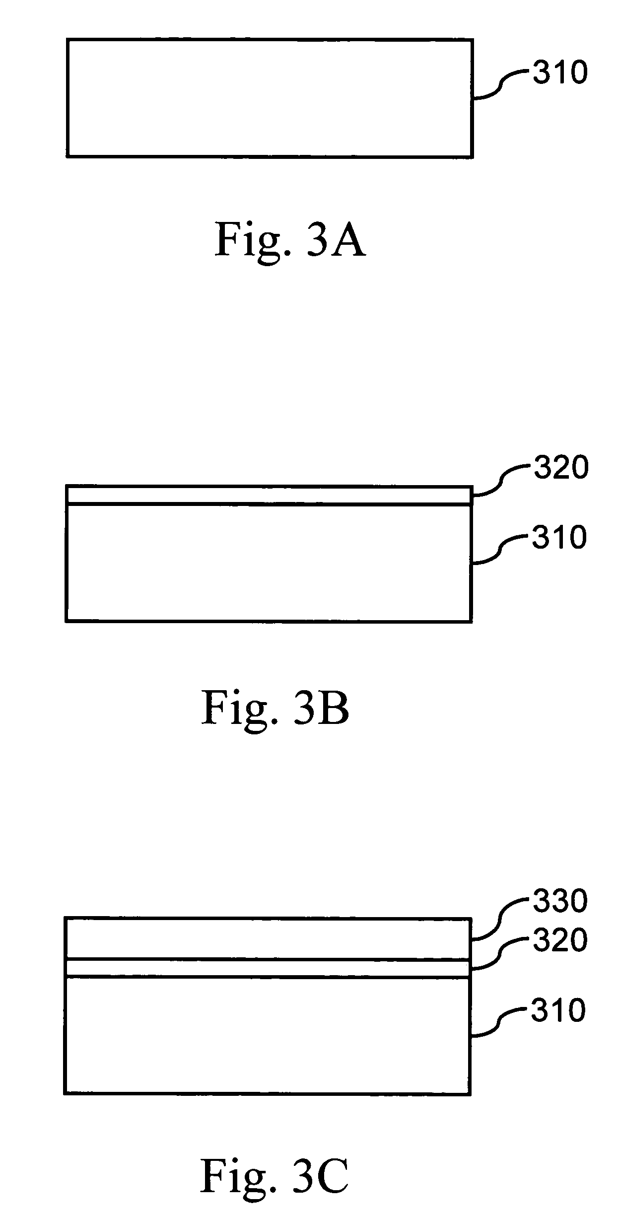
[0031]With reference to FIG. 3A to 3F, they are sectional views of the fabricating flow of the non-volatile memory device according to one embodiment of the present invention.

[0032]A...


PUM


Abstract

A non-volatile memory device and fabricating method thereof are provided. In the deposition to form a tunneling dielectric layer, a composite charge trapping layer and a block dielectric layer, an ingredient of a depositing material or the depositing material is adjusted to form a grading energy level structure, such that carriers are trapped or erased more easily in accordance with a variation in grading energy level. Therefore, the carriers are stored more effectively and the probability that the electric leakage occurs is reduced substantially.

Description

BACKGROUND[0001]1. Field of the Invention[0002]The present invention relates to a semiconductor memory device and fabricating method thereof, and more particularly to a non-volatile memory device and fabricating method thereof.[0003]2. Description of the Related Art[0004]Generally, semiconductor memory device may be classified into volatile memory device and non-volatile memory device. When power supply is interrupted, the data stored in the volatile memory device will disappear, while the data stored in the non-volatile memory device will still be stored. That is to say, the volatile memory device has the property that is the memory will disappear as the power is off. Therefore as the power supplied is discontinuous or interrupted frequently, or the element is an electronic element that requires low voltage only, such as memory card of the digital camera, portable disk, mobile phone, the non-volatile memory device is commonly used to store the data. As a result, the non-volatile me...

Claims


Application Information

Patent Timeline
Patent Type & Authority Patents(United States)
IPC IPC(8): H01L29/788
CPCH01L21/28273H01L21/28282H01L29/42324H01L29/4234H01L29/7881H01L29/792H01L29/40114H01L29/40117
Inventor LIN, CHA-HSINLEE, LURNG-SHEHNGTZENG, PEI-JER
Owner IND TECH RES INST
Why Eureka
Try Eureka