Semiconductor laser drive control device
a technology of laser drive and control device, which is applied in the direction of digitally marking record carriers, visual presentation using printers, instruments, etc., can solve the problems of deteriorating image quality, reducing light amount, and linearity of laser emission, so as to improve gradation characteristics
- Summary
- Abstract
- Description
- Claims
- Application Information
AI Technical Summary
Benefits of technology
Problems solved by technology
Method used
Image
Examples
embodiment 1
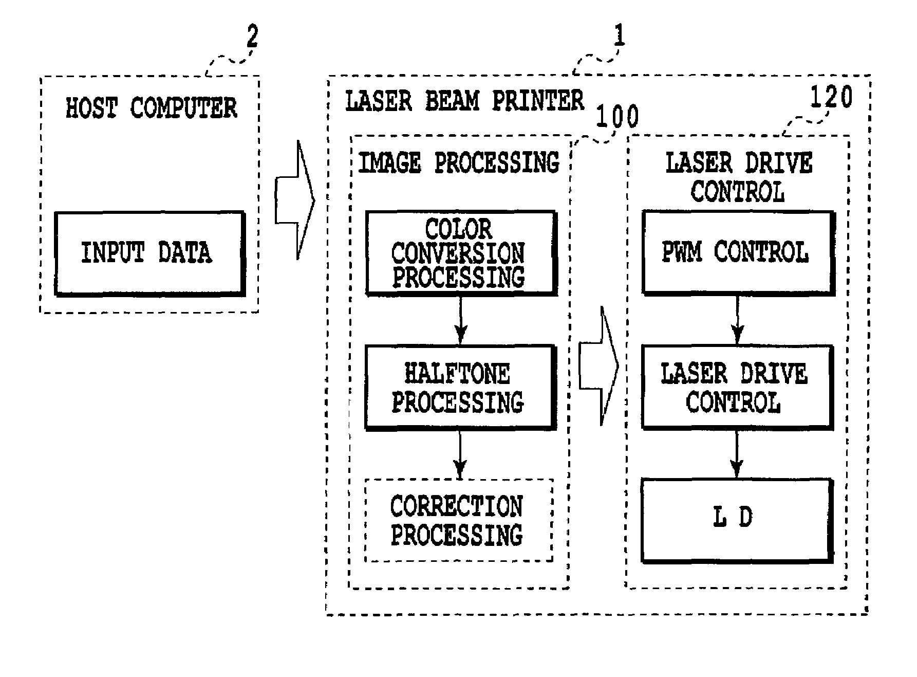
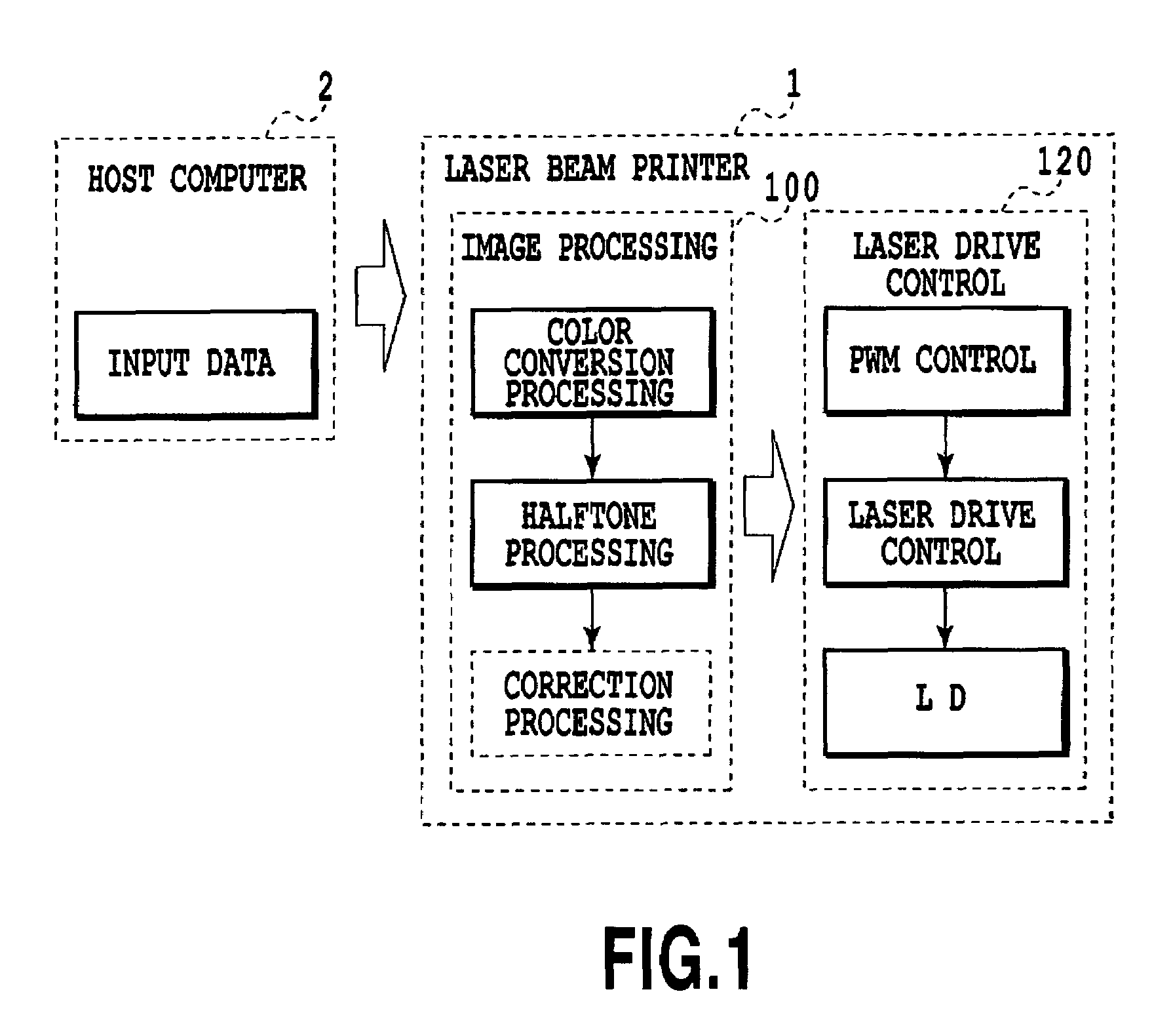
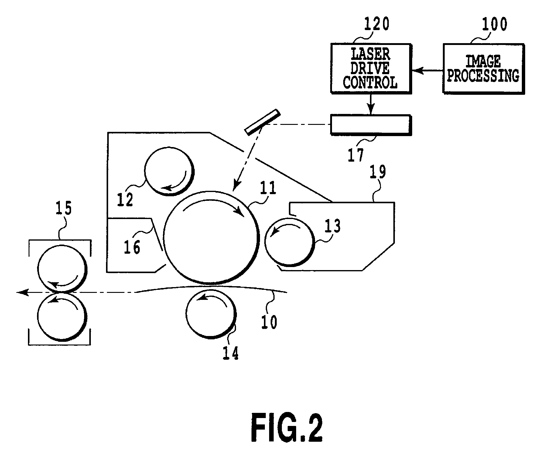
[0061]FIG. 1 illustrates a first embodiment of the present invention. This is an example of a laser beam printer which is shown in FIG. 2.
[0062]In FIG. 1, the reference numeral 1 represents the laser beam printer, which employs a pulse width modulation (PWM) system as the system for converting multivalued data into an amount of irradiating light and comprises an image processing 100 and a laser drive control 120. The image processing 100 performs color conversion processing and halftone processing based on input data from a host computer 2 connected to the laser beam printer 1, and further performs correction processing. The laser drive control 120 performs a PWM control to drive and control a semiconductor laser based on the image data processed in the image processing 100.
[0063]Referring now to FIG. 2, an image carrier 11 may be a functional separation type consists of a double layered structure including a charge generation layer and a charge transport layer or a single layer typ...
embodiment 2
[0097]The second embodiment of the present invention is now described.
[0098]A technique for correcting emission characteristics of a semiconductor laser, according to this embodiment, is first described. As shown in FIG. 20, an amount of emitting light (Laser Power) for each of input data of 00h to FFh (an index comprised of a hexadecimal number added with “h”, which specifies a concentration of a pixel) is measured when each pixel is PWM-driven with the same signal value. A result of plotting the amount of emitting light to the input data is shown in FIG. 21. A line indicated by “a” in the diagram exhibits a linear relationship of the amount of emitting light to the input data, and therefore is ideal. As shown in FIG. 22, if a pulse width for turning on the laser or turning off the laser is short, a response is not sufficient and therefore a light waveform is deformed. In such a case, as shown as a line indicated by “b” in FIG. 21, because the laser is not turned on in the highligh...
embodiment 3
[0106]FIG. 27 illustrates the third embodiment of the present invention. This embodiment is different from the first and second embodiments and on the point that the correction processing is performed with a host computer 2.
[0107]The correction processing in this embodiment is not essentially different from the procedure in the correction processing in FIG. 4 according to the first embodiment. A pixel distance and a time interval between a rising and a falling are detected from image data before correction and a PWM signal, and then the image data and the PWM signal are corrected with a correction amount appropriate to the obtained detection amount, followed by subsequent steps.
PUM
 Abstract
Description
Claims
Application Information
 - R&D
- Intellectual Property
- Life Sciences
- Materials
- Tech Scout
- Unparalleled Data Quality
- Higher Quality Content
- 60% Fewer Hallucinations
Browse by: Latest US Patents, China's latest patents, Technical Efficacy Thesaurus, Application Domain, Technology Topic, Popular Technical Reports.
© 2025 PatSnap. All rights reserved.Legal|Privacy policy|Modern Slavery Act Transparency Statement|Sitemap|About US| Contact US: help@patsnap.com


