Automatic calibration circuit for optoelectronic devices

a technology of optoelectronic devices and automatic calibration circuits, which is applied in automatic recalibration, measurement devices, instruments, etc., can solve the problems of time-consuming, expensive, and unreliable calibration performan

Active Publication Date: 2009-11-17
TEXAS ADVANCED OPTOELECTRONICS SOLUTIONS
View PDF10 Cites 16 Cited by
  • Summary
  • Abstract
  • Description
  • Claims
  • Application Information

AI Technical Summary

Problems solved by technology

However, this procedure is time consuming, expensive

Method used


Image

  • Automatic calibration circuit for optoelectronic devices
  • Automatic calibration circuit for optoelectronic devices
  • Automatic calibration circuit for optoelectronic devices

Examples


Embodiment Construction

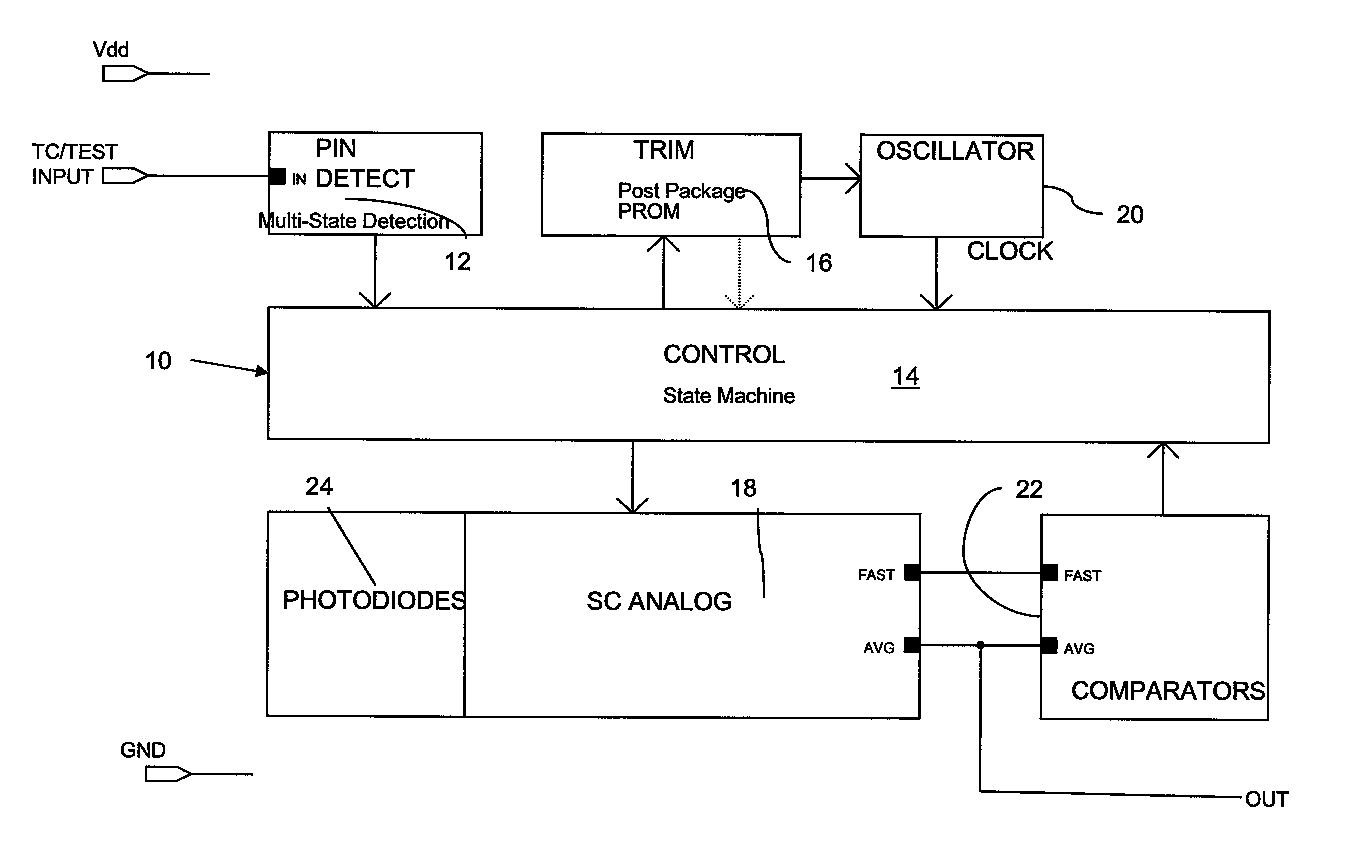
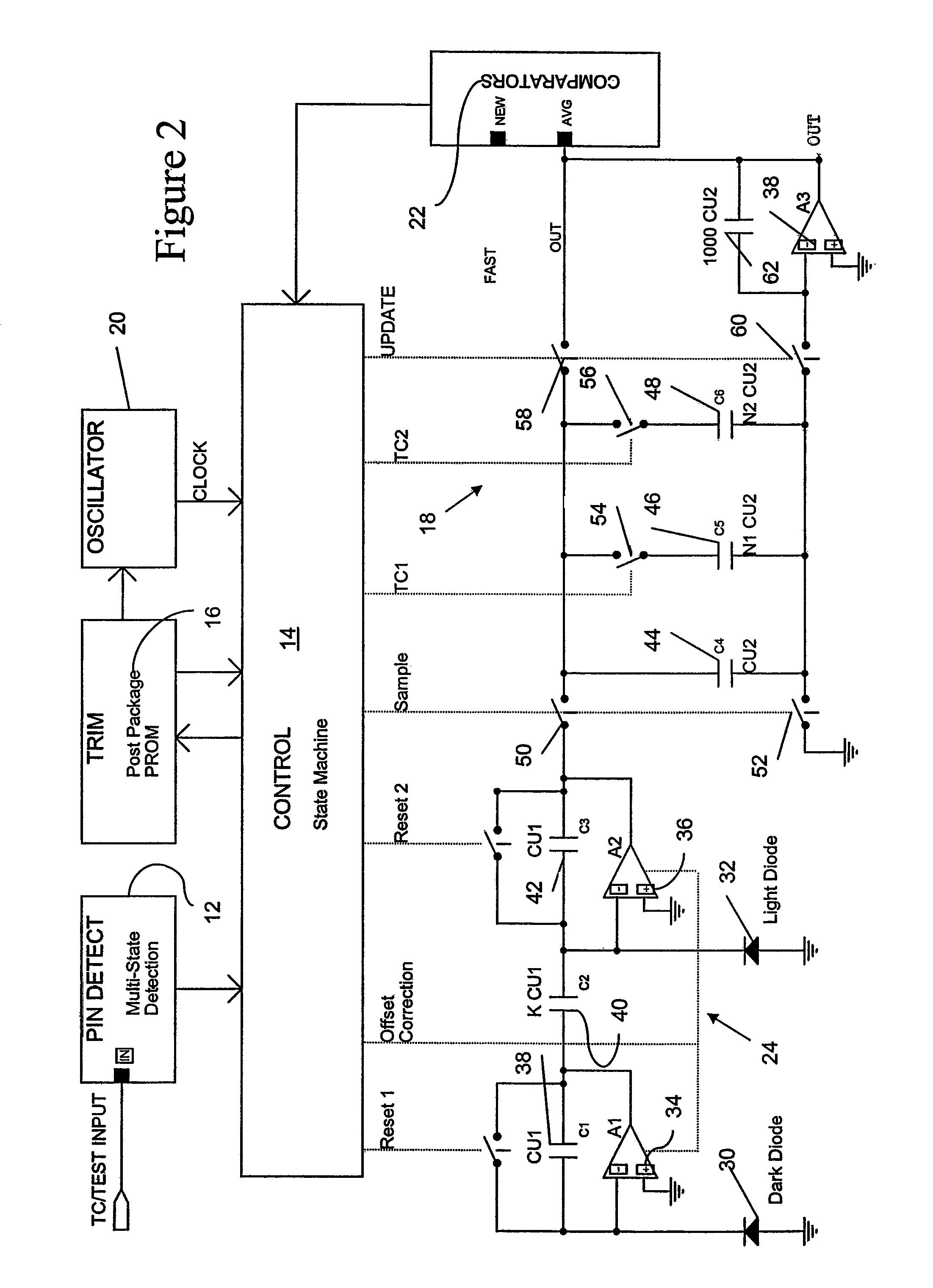
[0017]Referring simultaneously to FIGS. 1 and 2, the present automatic calibration circuit for use with optoelectronic devices is provided, and is generally identified by the numeral 10. Circuit 10 enables on-chip circuitry which permits the optoelectronic device to be calibrated post packaging, after installation in a target application. The present circuit 10 includes a calibration loop and programmable memory to enable calibration to be carried out in a simple and cost effective manner. The present circuit 10 ensures, that utilizing a known light source, a known response will be generated regardless of manufacturing tolerances of the optoelectronic device. The present circuit 10 enables repeatable performance and predictable results in view of manufacturing tolerances that influence various operational performance factors of the optoelectronic device.

[0018]Circuit 10 may be fabricated in a monolithic integrated circuit which utilizes both analog and mixed signal techniques, howev...


PUM


Abstract

A circuit for calibrating optoelectronic devices automatically trims a light sensor based upon a known light condition.

Description

RELATED APPLICATION[0001]This application claims the benefit of U.S. Provisional patent application Ser. No. 60 / 665,854 filed Mar. 29, 2005 and entitled “Integrated Analog Light Sensor with Adjustable Adaptive Response Speed and Internal Closed Loop Calibration Capability.”TECHNICAL FIELD OF THE INVENTION[0002]The present invention relates to optoelectronic devices, and more particularly to an automatic calibration circuit for optoelectronic devices.BACKGROUND OF THE INVENTION[0003]Optoelectronic devices, generally include devices that generate and transmit light, amplify light, detect light and control light. Such devices include, for example, ambient light sensors, color control sensors and color temperature sensors. Optoelectronic devices include components which are subject to manufacturing tolerances which cause variations in operational performance. It is therefore necessary to utilize calibration circuitry to compensate for variations in unit to unit performance and manufactu...

Claims


Application Information

Patent Timeline
IPC IPC(8): G02B6/00
CPCG01D18/004
Inventor ASWELL, CECIL
Owner TEXAS ADVANCED OPTOELECTRONICS SOLUTIONS
Why Eureka
Try Eureka