
Device and method to eliminate step response power supply perturbation

a step response and power supply technology, applied in the field of voltage island devices, can solve the problems of step response, voltage gradient, step response remains a serious problem, and the voltage at the operating circuit is reduced relativ

Inactive Publication Date: 2009-03-31
GLOBALFOUNDRIES INC
View PDF6 Cites 11 Cited by
  • Summary
  • Abstract
  • Description
  • Claims
  • Application Information

AI Technical Summary

Benefits of technology

[0023]In a related aspect of the present invention the control decoder prevents disabling the secondary header on the voltage island and near simultaneously enabling the primary header on the voltage island during a period when noise is on the secondary header or the secondary voltage is not substantially equal to the primary voltage.
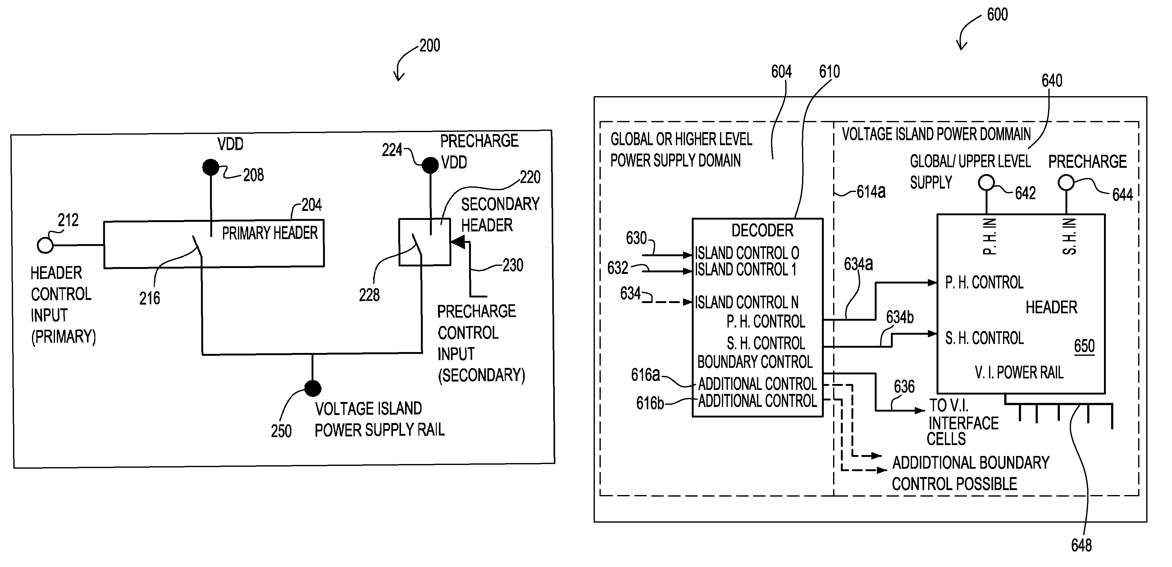
[0024]In a further aspect of the present invention, a method is provided for eliminating step response power supply perturbation during voltage island power-up / power-down on an integrated circuit. The method comprises the steps of providing an IC chip communicating with a primary power supply, and the IC chip including at least one voltage island. Providing a primary header on the voltage island of the chip, where the primary header communicates with the primary power supply via a primary header power path. Providing a secondary header on the voltage island of the chip where the secondary header communicates with a secondary power supply via a secondary header power path. Providing a control decoder communicating with the IC chip and the at least one voltage island. The method further comprises the steps of requesting an initial power-up of the voltage island, and enabling the secondary header using the control decoder. The secondary header is then disabled using the control decoder, and the primary header is enabled using the control decoder.

Problems solved by technology

IR drop is caused by the DC current demand of the Integrated Circuit (IC) and resistance of the power supply network within the IC and results in both reduced voltage at the operating circuits relative to the voltage supplied at IC level and voltage gradients across the IC.
However, step response remains a serious problem in today's IC chips because voltage extremes produced during the step response dictate the minimum and maximum operating voltages encountered within an IC.
However switching of the VI power supply places the IC at risk of failure due to step response voltage transients and their inherent oscillation frequencies.
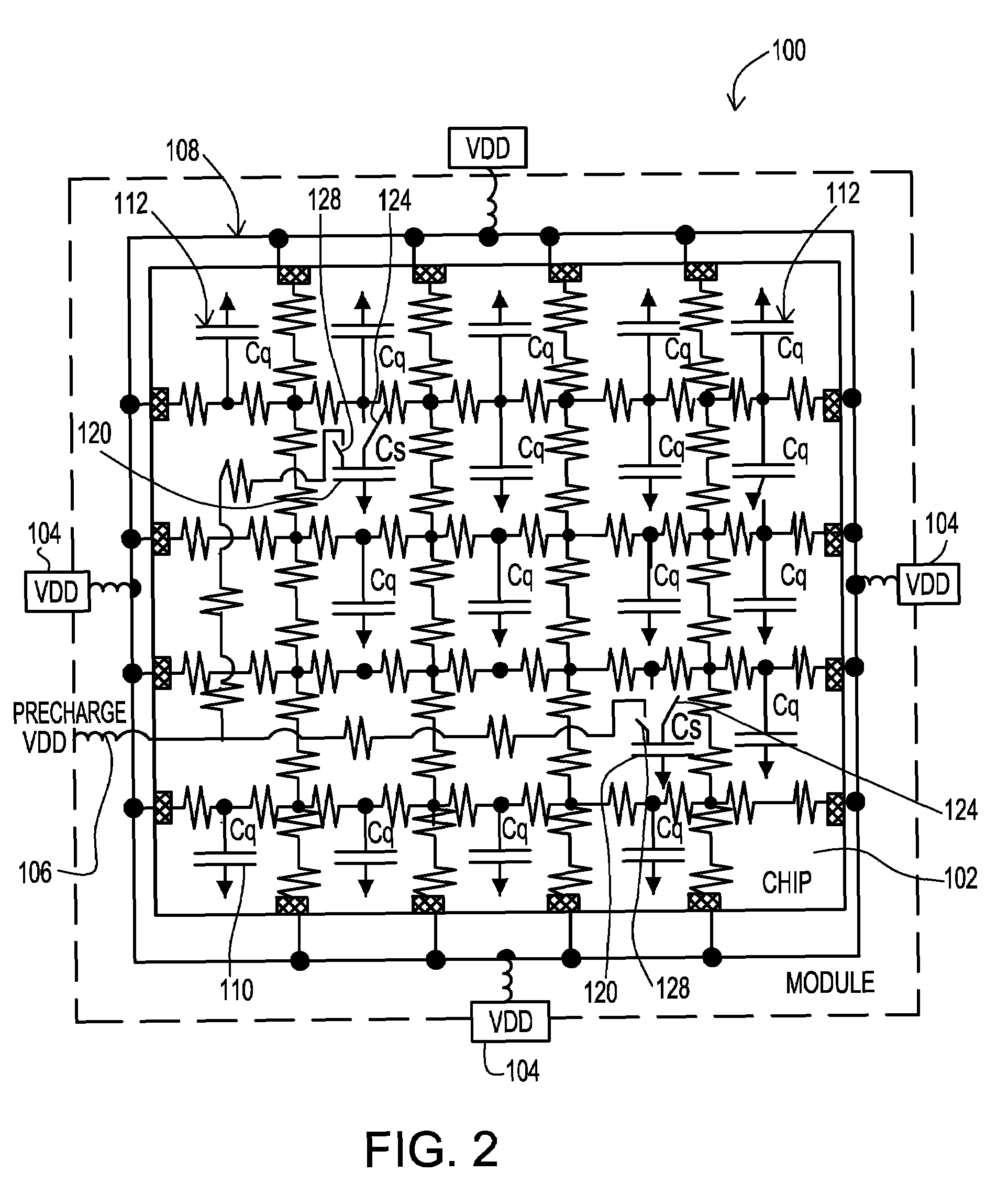
These sudden changes in current requirements generate a step response in the chip-package power bus network which results in damped ringing of the power bus voltage, i.e., power supply perturbation.
Thus, an undesirable step response results which produces unwanted power supply perturbation.
These frequencies are centered around clock frequencies typically encountered in ICs for both data processing and I / O functions which further compromises functionality of the IC as the voltage oscillation affects path delays within the IC from cycle to cycle.
Past IC chip designs have been unable to adequately resolve the undesirable step response issue.
These challenges require even more attention to power distribution in the chip and the affects of step response perturbation at each new technology node.
Design of these structures is complex and may not always optimize turn-on time for the internal capacitance of the voltage island.
Thus, typical header circuits have not been successful in mitigating RLC-induced power supply ringing caused by current step response during voltage island power-up / power-down.

Method used


Image

  • Device and method to eliminate step response power supply perturbation
  • Device and method to eliminate step response power supply perturbation
  • Device and method to eliminate step response power supply perturbation

Examples


Embodiment Construction

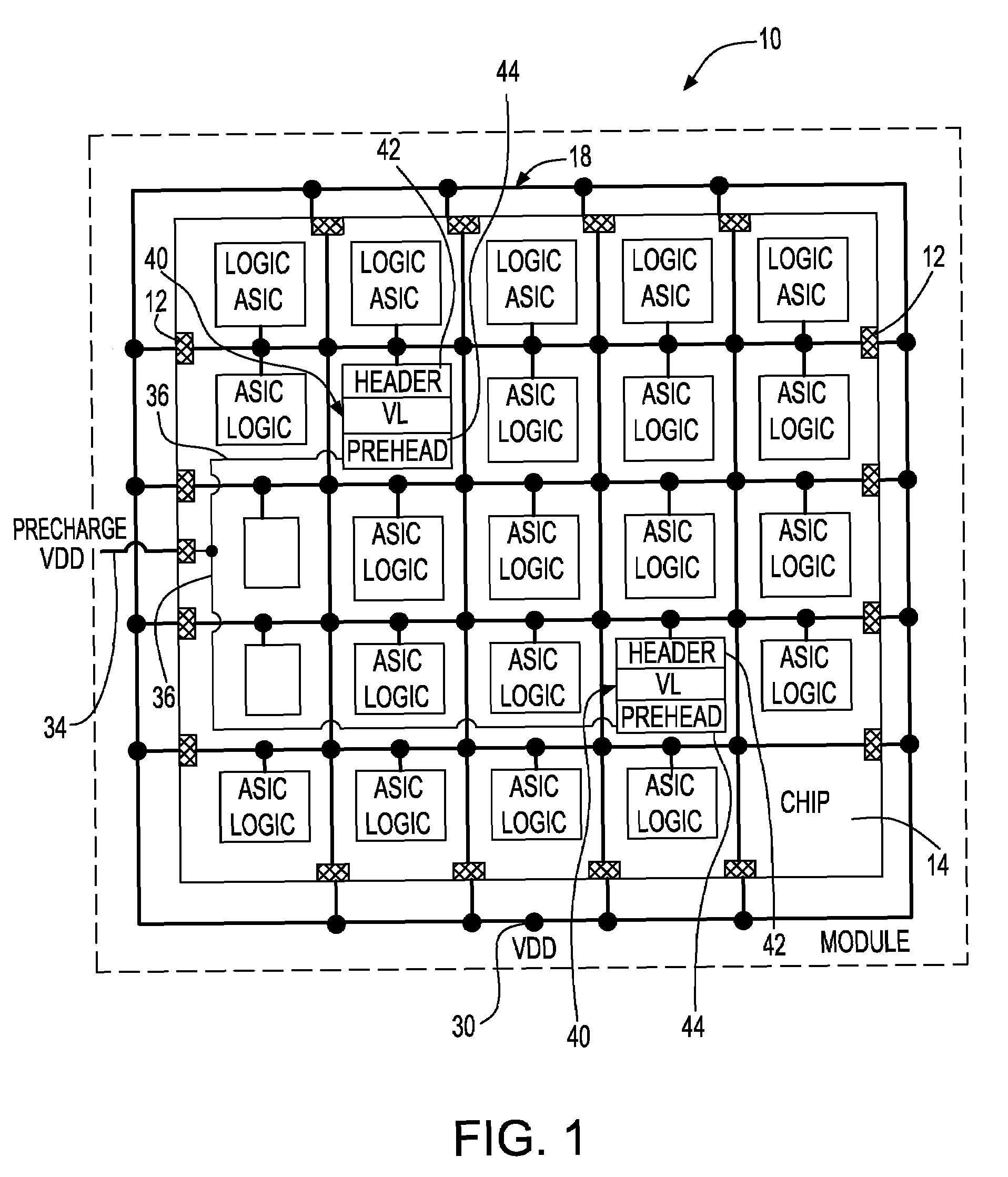
[0039]The present invention provides a new header design and image / package bus plan which eliminates the voltage island power-up issue of a step response during power up (di / dt) resulting in power supply perturbation. In addition, the present invention results in both efficient management of voltage island power state transition and efficient central management of voltage island power up. Further, the present invention teaches a topology for mitigation of island power-off (di / dt) transient mitigation.

[0040]The present invention provides a power on methodology for an IC voltage island having primary and secondary header circuits where the secondary header circuit is enabled and the island is pre-charged / repowered in a static mode. Then, the secondary header is disabled and the primary header is enabled to provide connectivity to a power bus with functional current-load capability. Finally, the island data / clock boundaries are enabled to start IC functional processing.

[0041]Referring ...


PUM


Abstract

A system and method for eliminating step response power supply perturbation during voltage island power-up / power-down on an integrated circuit is disclosed. An IC chip communicates with a primary power supply and includes at least one voltage island. A primary header on the voltage island of the chip communicates with the primary power supply via a primary header power path. A secondary header on the voltage island of the chip communicates with a secondary power supply via a secondary header power path. A control decoder communicating with the IC chip and the voltage island regulates the state of the primary and secondary headers.

Description

FIELD OF THE INVENTION[0001]The invention relates to a voltage island device on an integrated circuit, and more particularly, to a voltage island device for eliminating step response power supply perturbation during voltage island power-up / power down.BACKGROUND OF THE INVENTION[0002]Three principle sources of power supply perturbation exist within today's integrated circuits: resistive voltage (IR) drop; cyclic power supply ripple; and DI / DT induced supply bus ringing. IR drop is caused by the DC current demand of the Integrated Circuit (IC) and resistance of the power supply network within the IC and results in both reduced voltage at the operating circuits relative to the voltage supplied at IC level and voltage gradients across the IC. Cyclic power supply ripple is generated by clocked logic operating on the IC which creates periodic AC current variation and resultant voltage ripple. DI / DT induced supply bus ringing is caused by near-instantaneous current demand changes during IC...

Claims


Application Information

Patent Timeline
Patent Type & Authority Patents(United States)
IPC IPC(8): H03K17/16H03K19/003
CPCH03K19/00346
Inventor ARSOVSKI, IGORIADANZA, JOSEPH A.
Owner GLOBALFOUNDRIES INC
Learn More