Microminiature power converter and thin film magnetic induction device thereof
a technology of micro-miniature power converter and induction device, which is applied in the direction of semiconductor devices, transformer/inductance details, basic electric elements, etc., can solve the problems of increasing manufacturing costs, reducing packaging area of power modules, and occupying a significant amount of magnetic parts in comparison with integrated circuits, so as to reduce the induced voltage
- Summary
- Abstract
- Description
- Claims
- Application Information
AI Technical Summary
Benefits of technology
Problems solved by technology
Method used
Image
Examples
first embodiment
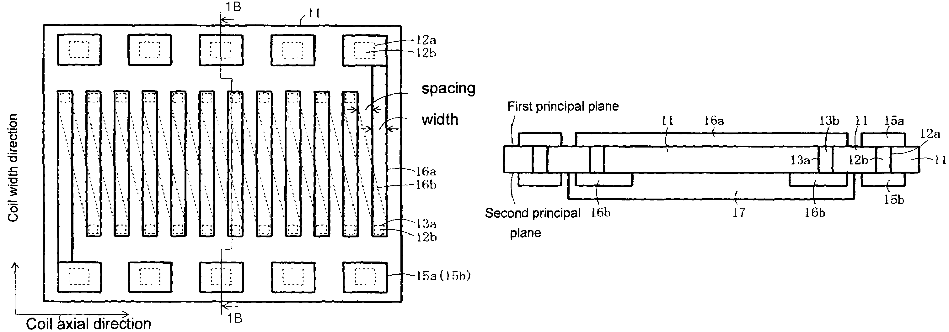
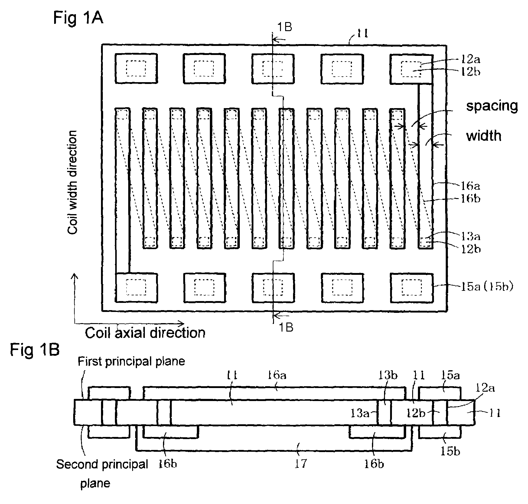
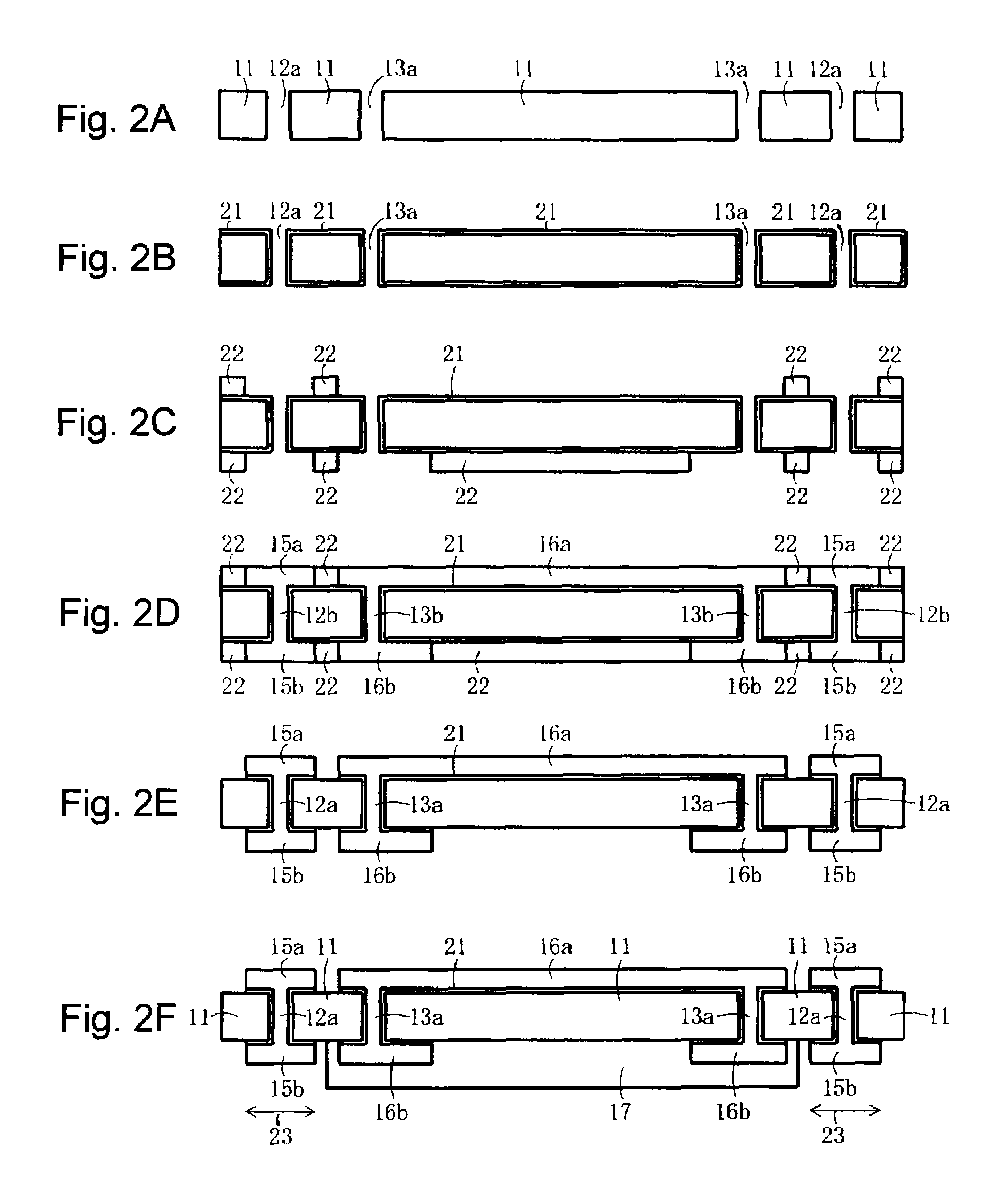
[0031]Referring to FIGS. 1A and 1B, although the microminiature power converter includes an IC chip and other components, as shown in FIG. 11, they are omitted in FIGS. 1A and 1B to show the thin film magnetic induction device. The thin film magnetic induction device comprises a ferrite substrate 11, which is a magnetic insulating substrate, a solenoid coil formed in the inner region of the ferrite substrate 11, pairs of electrodes arranged in the peripheral side region of the ferrite substrate 11 along the direction parallel to the axis of the coil, pairs of electrodes 15a and 15b opposing one another while sandwiching the ferrite substrate 11, and a protective film 17. The solenoid coil includes coil conductors 16a and 16b, and connection conductors 13b that electrically connect the coil conductors 16a and 16b to form a coil configuration. Connection conductors 12b electrically connect the electrodes 15a and 15b. The connection conductors 12b and 13b are provided by forming conduc...
third embodiment
[0053]In the alternative embodiment of FIGS. 6A and 6B, the electrodes 15a, 15b are drawn inwardly from the outer peripheral end. However, as provided in the third embodiment, the electrodes 15a, 15b can extend to the outer peripheral end without negating the advantages.
[0054]FIGS. 8A, 8B, 8C show the fourth embodiment of a microminiature power converter. In the fourth embodiment, a groove 70 with a slit shape that does not pass throughout the ferrite substrate 11 extends from the through-hole 12a connecting the electrode 15a on the first principal plane and the electrode 15b on the second principal plane to the outer peripheral end of the substrate. Thus, part of the ferrite substrate 11 outside the electrodes 15a, 15b is decreased, thereby reducing the outer peripheral magnetic flux 43 flowing outside the electrodes 15a, 15b. To fabricate the fourth embodiment, again, only the patterning step (FIG. 2A) of forming the through-holes in the ferrite substrate in the steps (FIGS. 2A-2F...
PUM
| Property | Measurement | Unit |
|---|---|---|
| thickness | aaaaa | aaaaa |
| width | aaaaa | aaaaa |
| thickness | aaaaa | aaaaa |
Abstract
Description
Claims
Application Information
 - R&D
- Intellectual Property
- Life Sciences
- Materials
- Tech Scout
- Unparalleled Data Quality
- Higher Quality Content
- 60% Fewer Hallucinations
Browse by: Latest US Patents, China's latest patents, Technical Efficacy Thesaurus, Application Domain, Technology Topic, Popular Technical Reports.
© 2025 PatSnap. All rights reserved.Legal|Privacy policy|Modern Slavery Act Transparency Statement|Sitemap|About US| Contact US: help@patsnap.com


