Method for forming nanostructured carbons, nanostructured carbons and a substrate having nanostructured carbons formed thereby
a technology of nanostructured carbons and nanostructured carbons, which is applied in the field of nanostructured carbons formation methods, can solve the problems of increasing equipment expenses and production costs, complex equipment, and difficult to make nanostructured carbons directly grown on a planar substrate in the arc-discharge process, and achieves the effect of easy and fast formation
- Summary
- Abstract
- Description
- Claims
- Application Information
AI Technical Summary
Benefits of technology
Problems solved by technology
Method used
Image
Examples
example 1
[0109]Process of Attaching Fine Metal Particles to Substrate Surfaces
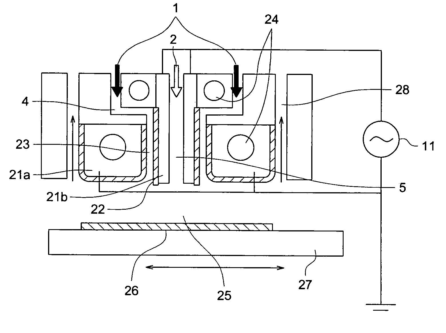
[0110]We attached fine metal particles to substrate surfaces by using equipment having a configuration of FIG. 5.
[0111]We prepared pure-iron (Fe) targets of 20 mm×20 mm×120 mm (long) as the electrodes 21a and 21b. Each target had its edges rounded (R3) and contained a through-hole through which silicone oil flowed to control the electrode temperature by heat exchange.
[0112]The moving stage electrode 27 was made of a titanium plate (JIS Class 2 titanium) of 100 mm×500 mm×20 mm and had three through-holes to control the electrode temperature. The surface of this electrode was coated with alumina ceramic by thermal spraying to have a ceramic coat of 0.8 mm thick. Then a dielectric layer 22 was formed on the alumina ceramic layer of the stage electrode by applying an organic solution of alkoxysilane monomer to the alumina ceramic layer, drying thereof, and sealing thereof at 300° C.
[0113]We arranged two of the above ta...
example 2
[0124]Example of using a Substrate having a Conductive Layer on it
[0125]The metal particle attaching process and the nanostructured carbon fabricating process of this example are the same as those of Example 1 but Example 2 uses a substrate having a conductive layer on it. Example 2 could also get carbon materials of carbon nanotubes almost similar to those obtained by Example 1. A conductive layer was formed on the substrate as follows:
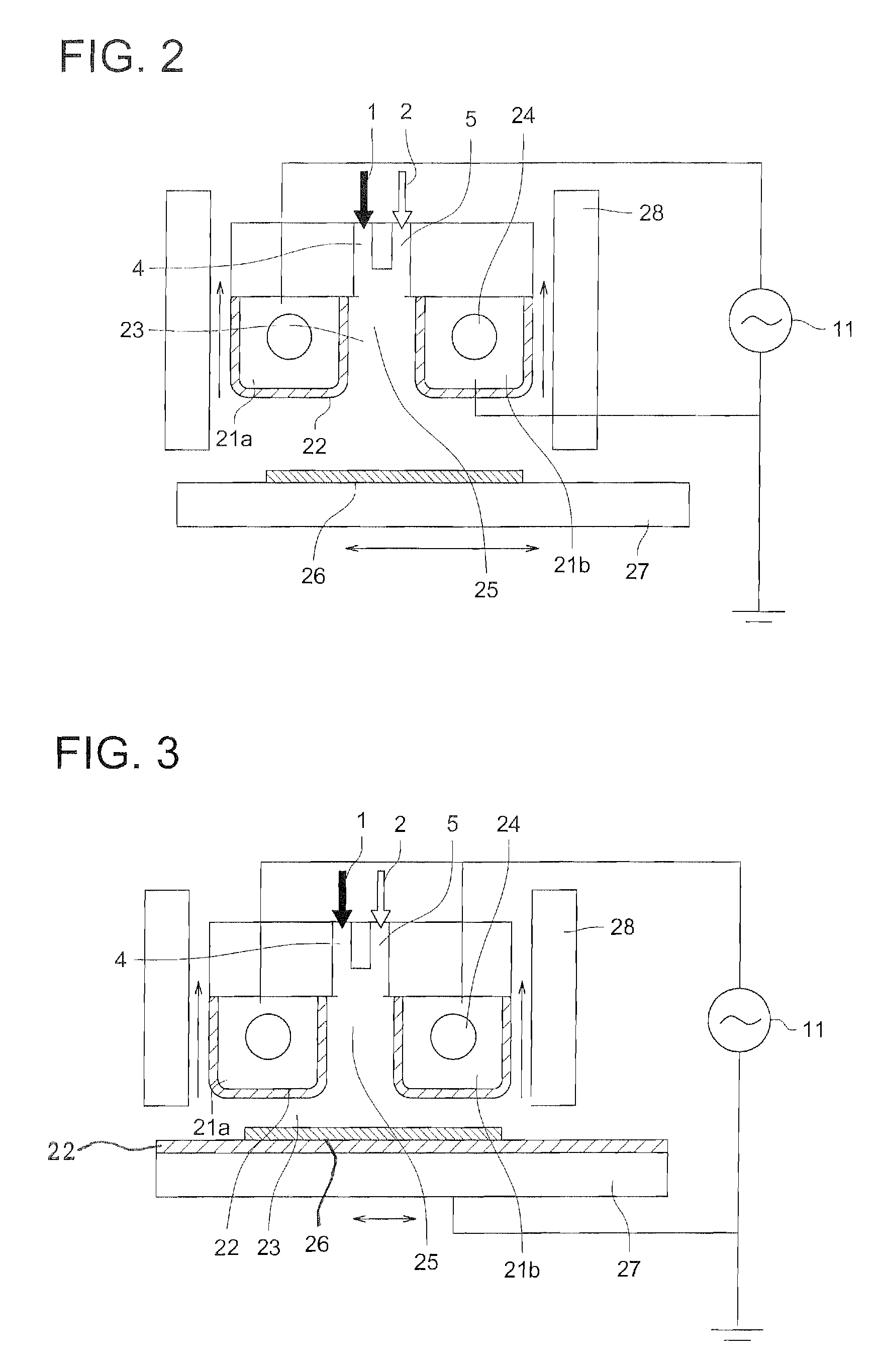
[0126]We placed a base material on the moving stage electrode 27 in the equipment of FIG. 5 (having electrodes coated with dielectric material) and purged the gas in the container with nitrogen gas until the concentration of oxygen gas in the container becomes 50 ppm.
[0127]We fed a mixture gas of 95.9% by volume of nitrogen gas, 0.1% by volume of aluminum acetyl acetate vapor, and 4% by volume of hydrogen gas into the equipment and applied a high frequency voltage of 50 kHz, 8 KV to one of the electrodes and a high frequency voltage of 13.56 MHz, 8 w...
example 3
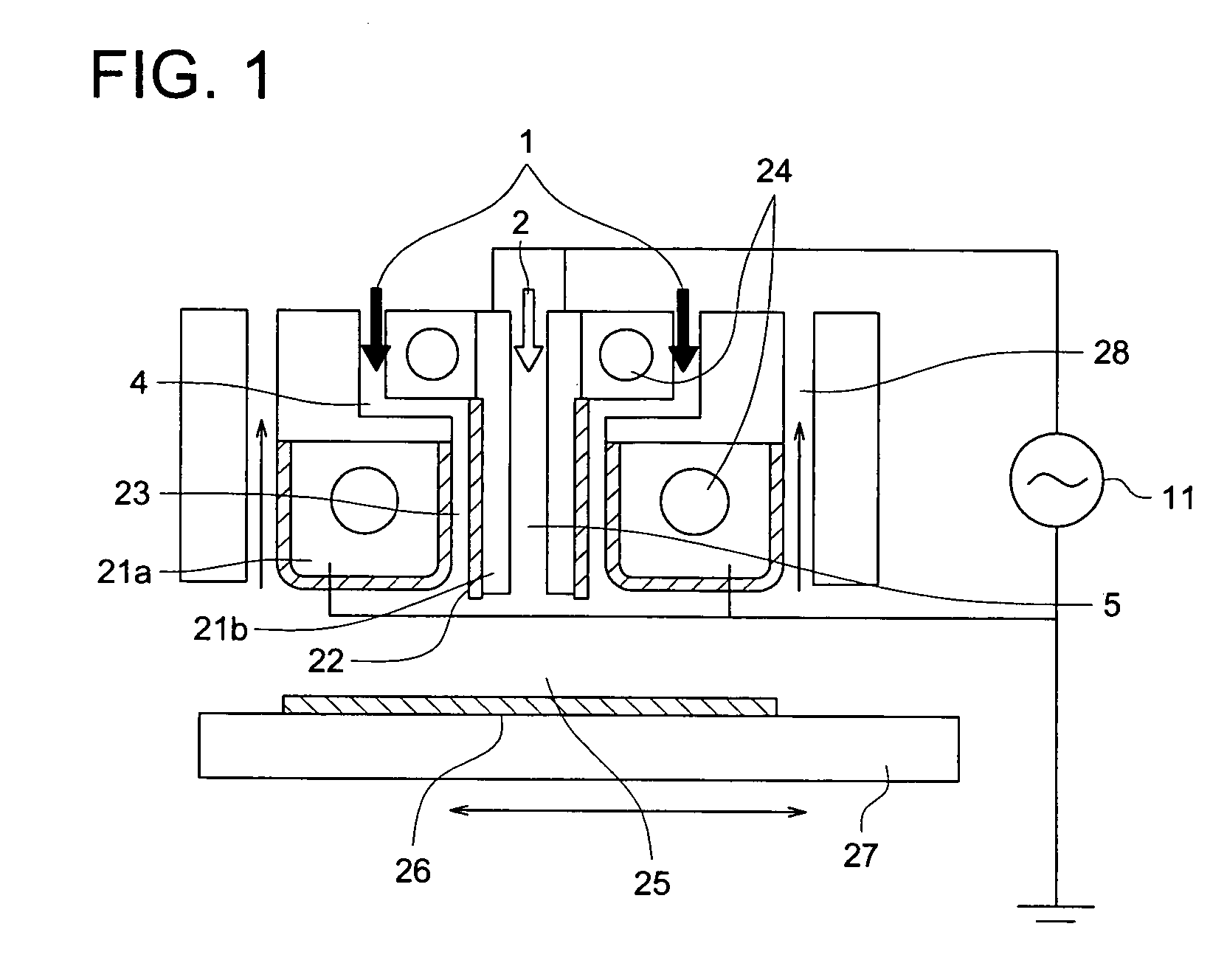
[0132]We formed nanostructured carbons on a substrate having a conductive layer on it in the manner similar to Example 1 by using the equipment configuration of FIG. 4.
[0133]We prepared, as electrodes 21a and 21b, titanium bars (JIS Class 2 titanium) of 20 mm×20 mm×120 mm (long). Each electrode bar had its edges rounded (R3) and contained a through-hole for heat exchange. The surface of each electrode bar was coated with alumina ceramic by thermal spraying to have a ceramic coat of 0.8 mm thick. Then a dielectric layer 22 was formed on the alumina ceramic layer of each electrode bar by applying an organic solution of alkoxysilane monomer to the alumina ceramic layer, drying thereof, and sealing thereof at 300° C.
[0134]We arranged two of the above electrode bars to form a clearance of 2 mm wide between them so that the raw material gas containing the discharge gas might flow through this clearance. We used the same moving stage electrode 27 as what was prepared for the metal particle...
PUM
| Property | Measurement | Unit |
|---|---|---|
| frequency | aaaaa | aaaaa |
| temperature | aaaaa | aaaaa |
| atmospheric pressure | aaaaa | aaaaa |
Abstract
Description
Claims
Application Information
 - R&D
- Intellectual Property
- Life Sciences
- Materials
- Tech Scout
- Unparalleled Data Quality
- Higher Quality Content
- 60% Fewer Hallucinations
Browse by: Latest US Patents, China's latest patents, Technical Efficacy Thesaurus, Application Domain, Technology Topic, Popular Technical Reports.
© 2025 PatSnap. All rights reserved.Legal|Privacy policy|Modern Slavery Act Transparency Statement|Sitemap|About US| Contact US: help@patsnap.com


