Dynamic random access memory structure
a random access and memory technology, applied in the direction of semiconductor devices, electrical devices, transistors, etc., can solve the problems of the retention time of the carriers, and achieve the effects of increasing integration, reducing the area of the storage device, and prolonging the retention tim
- Summary
- Abstract
- Description
- Claims
- Application Information
AI Technical Summary
Benefits of technology
Problems solved by technology
Method used
Image
Examples
Embodiment Construction
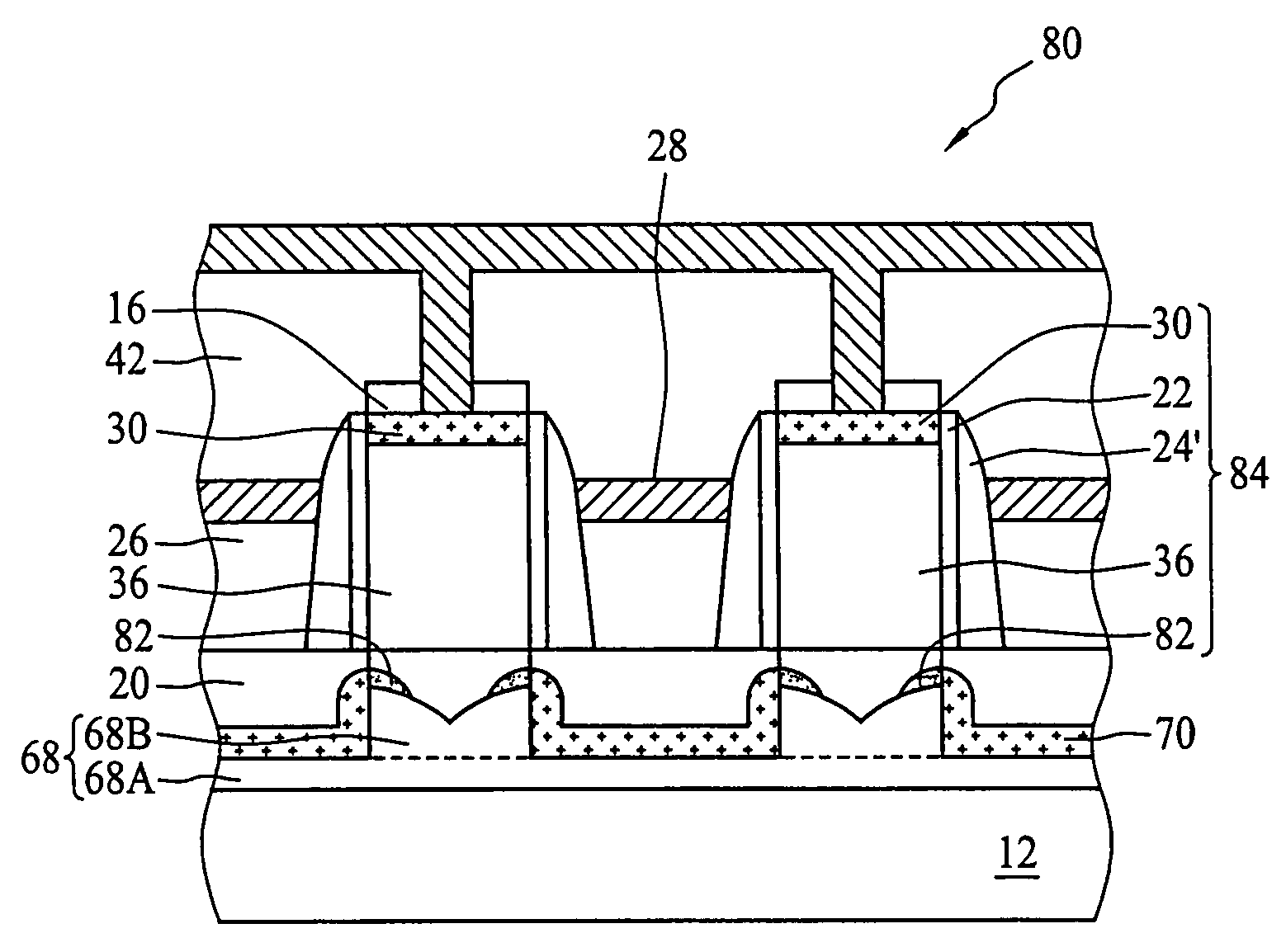
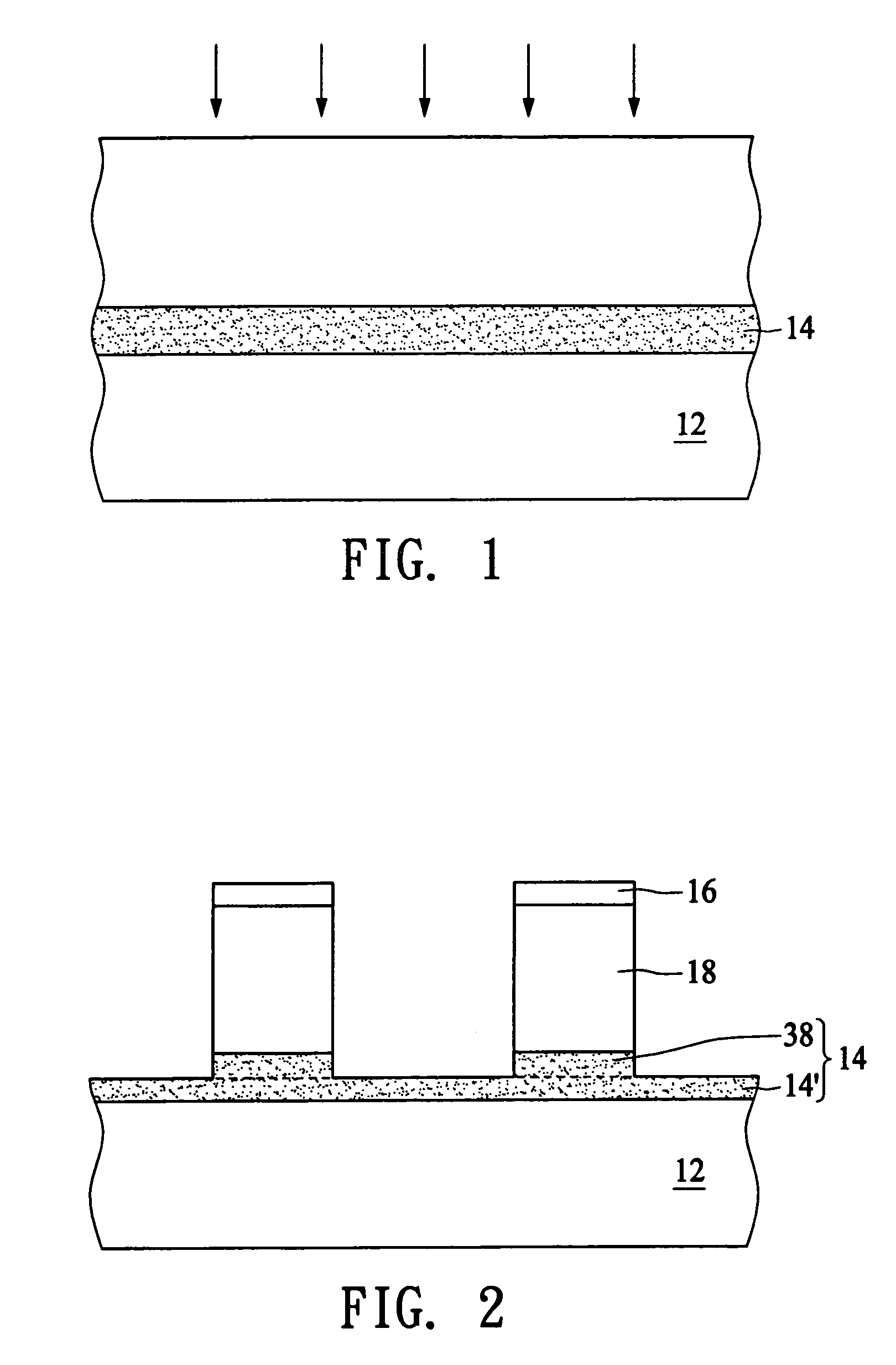
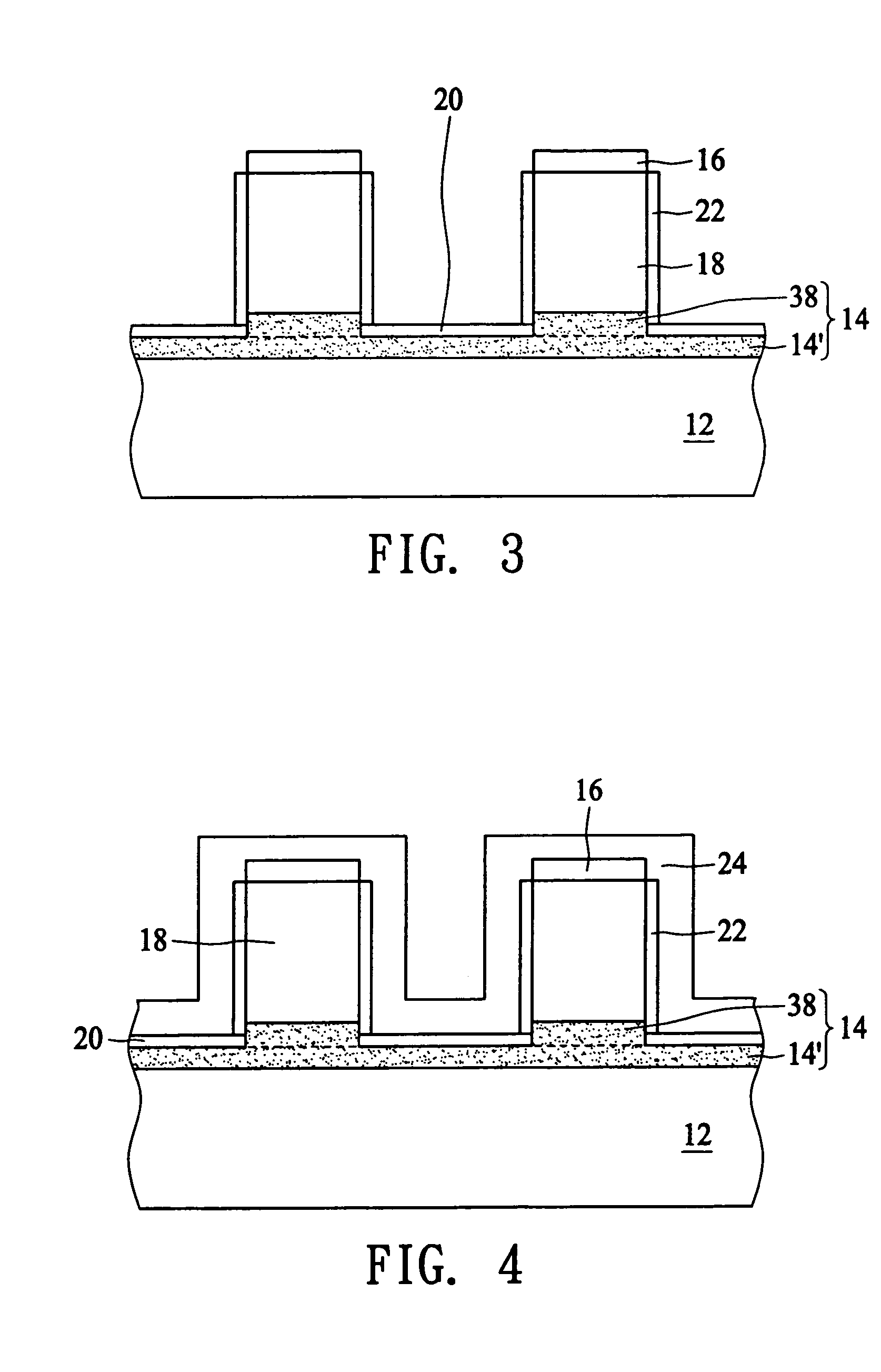
[0017]FIG. 1 to FIG. 6 illustrate a method for preparing a dynamic random access memory structure 10 according to one embodiment of the present invention. First, an implanting process is performed to implant ions into a predetermined depth in a semiconductor substrate 12 such as a silicon substrate to form a conductive layer 14 in the semiconductor substrate 12. Subsequently, a mask layer 16 is formed on the semiconductor substrate 12 and an etching process is then performed to remove a portion of the semiconductor substrate 12 not covered by the mask layer 16 down to the interior of the conductive layer 14 in the semiconductor substrate 12 to form a plurality of cylindrical pillars 18. Particularly, the conductive layer 14 can be regarded as two portions, i.e., a bottom conductive region 38 at the bottom portion of the cylindrical pillar 18 and a conductive layer 14′ on the surface of the semiconductor substrate 12, as shown in FIG. 2.
[0018]Referring to FIG. 3, a deposition process...
PUM
 Abstract
Description
Claims
Application Information
 - R&D
- Intellectual Property
- Life Sciences
- Materials
- Tech Scout
- Unparalleled Data Quality
- Higher Quality Content
- 60% Fewer Hallucinations
Browse by: Latest US Patents, China's latest patents, Technical Efficacy Thesaurus, Application Domain, Technology Topic, Popular Technical Reports.
© 2025 PatSnap. All rights reserved.Legal|Privacy policy|Modern Slavery Act Transparency Statement|Sitemap|About US| Contact US: help@patsnap.com


