
Active-matrix substrate and display device including the substrate wherein a bottom-gate TFT has data lines formed below the gate lines

a technology of active matrix and substrate, which is applied in the field of active matrix substrate and display device, can solve the problems of deteriorating display quality, increasing the size and definition of lcds, and high demand for lcds, so as to reduce the capacitance produced, reduce the drivability of switching elements, and reduce the resistance of wiring.

Active Publication Date: 2008-10-14
MERCK PATENT GMBH
View PDF13 Cites 7 Cited by
  • Summary
  • Abstract
  • Description
  • Claims
  • Application Information

AI Technical Summary

Benefits of technology

[0010]In order to overcome the problems described above, an object of the present invention is to provide an active-matrix substrate that can reduce the capacitance produced in the intersections between the gate lines and source lines without increasing the wiring resistance or decreasing the drivability of switching elements, and also provide a display device including such an active-matrix substrate.
[0032]According to a preferred embodiment of the present invention, source lines are provided under gate lines with a first interlayer insulating film interposed between them and are electrically connected to the source electrodes of thin-film transistors through contact holes that have been cut through the first interlayer insulating film. Thus, in an active-matrix substrate including thin-film transistors of a bottom-gate type, the capacitance produced in the intersections between the gate lines and source lines can be reduced without increasing the wiring resistance or decreasing the drivability of the thin-film transistors.

Problems solved by technology

The capacitance produced in each gate line-source line intersection (which is usually called a “parasitic capacitance”) may cause some deterioration in display quality.
Also, if the line widths were decreased, then the chances of line snapping would increase.
However, the sizes and definitions of LCDs in high demand have been on a steep rise recently.
However, if a portion of the insulating film that covers the gate line function as a gate insulating film as in a bottom-gate TFT, the thickened insulating film would decrease the drivability of the TFT.

Method used


Image

  • Active-matrix substrate and display device including the substrate wherein a bottom-gate TFT has data lines formed below the gate lines
  • Active-matrix substrate and display device including the substrate wherein a bottom-gate TFT has data lines formed below the gate lines
  • Active-matrix substrate and display device including the substrate wherein a bottom-gate TFT has data lines formed below the gate lines

Examples


embodiment 1

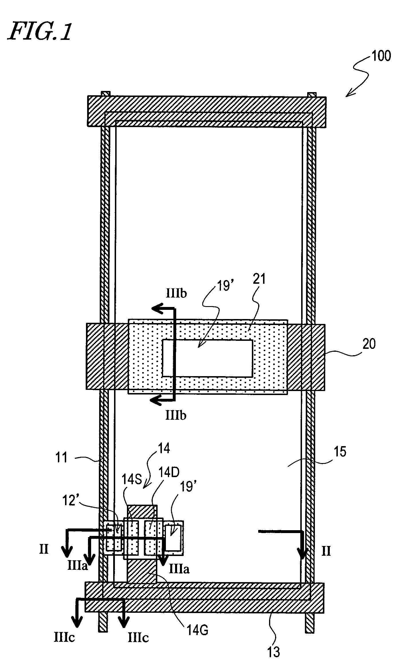
[0051]FIGS. 1 and 2 illustrate an LCD 100 according to a first specific preferred embodiment of the present invention. FIG. 1 is a plan view schematically illustrating one pixel region of the LCD 100. FIG. 2 is a cross-sectional view of the LCD 100 as viewed on the plane II-II shown in FIG. 1.

[0052]The LCD 100 includes an active-matrix substrate 100a (which will be referred to herein as a “TFT substrate 100a”), a counter substrate 100b (which will be sometimes referred to herein as a “color filter substrate 100b”) that faces the TFT substrate 100a , and a liquid crystal layer 60 interposed between the two substrates 100a and 100b.

[0053]The TFT substrate 100a preferably includes a transparent insulating substrate (e.g., a glass substrate) 10, a plurality of source lines 11 arranged on the substrate 10, a first interlayer insulating film 12 provided so as to cover the source lines 11, and a plurality of gate lines 13, which are provided on the first interlayer insulating film 12 so a...

embodiment 2

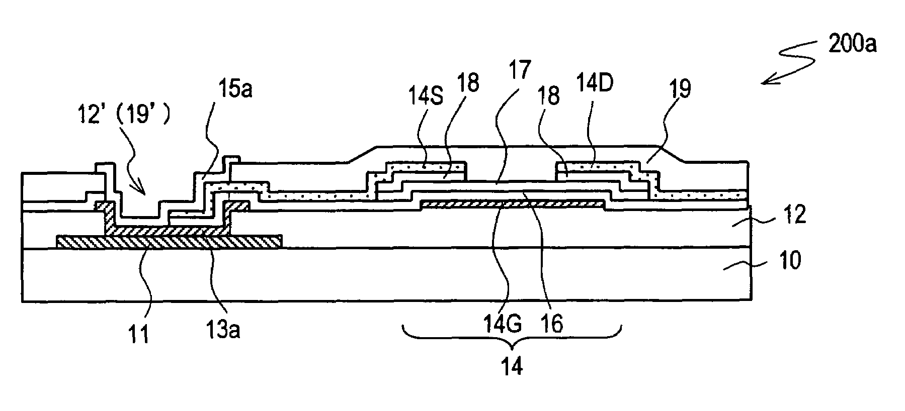
[0081]An LCD 200 according to a second specific preferred embodiment of the present invention will be described with reference to FIG. 5 and FIGS. 6A through 6C. The following description of the second preferred embodiment will be focused on the difference between the LCD 100 of the first preferred embodiment and the LCD 200 of the second preferred embodiment.

[0082]In the TFT substrate 200a of the LCD 200, the source line 11 and the source electrode 14S are connected together differently from the TFT substrate 100a of the first preferred embodiment. In the TFT substrate 100a, the source electrode 14S is directly in contact with the source line 11 within the contact hole 12′ of the first interlayer insulating film 12, thereby electrically connecting the source line 11 and the source electrode 14S together as shown in FIG. 3A.

[0083]On the other hand, the TFT substrate 200a further includes a first conductive member 13a formed by patterning the same conductive film as the gate lines 13...

embodiment 3

[0104]FIG. 11 and FIGS. 12A through 12D schematically illustrate an LCD 300 according to a third specific preferred embodiment of the present invention.

[0105]As shown in FIG. 11 and FIGS. 12A through 12C, the TFT substrate 300a of the LCD 300 of this preferred embodiment has almost the same configuration as the TFT substrate 200a of the LCD 200 of the second preferred embodiment described above.

[0106]However, unlike the TFT substrate 200a of the LCD 200, the TFT substrate 300a of the LCD 300 of this preferred embodiment includes a plurality of shield electrodes 23, extending substantially parallel to the source lines 11, as shown in FIGS. 11 and 12D.

[0107]In this preferred embodiment, the shield electrodes 23 are formed by patterning the same conductive film as the gate lines 13. These shield electrodes 23 are connected to the storage capacitor line 20 and are supplied with a constant potential. Hereinafter, problems that may happen without the shield electrodes 23 and advantages ac...


PUM

PropertyMeasurementUnit
thicknessaaaaaaaaaa
dielectric constantaaaaaaaaaa

Abstract

An active-matrix substrate includes: a base substrate; source lines; gate lines; thin-film transistors; and pixel electrodes. Each transistor is a bottom-gate thin-film transistor. The source lines are arranged under the gate lines with a first interlayer insulating film interposed and are electrically connected to the respective source electrodes of their associated thin-film transistors through contact holes cut through the first interlayer insulating film.

Description

BACKGROUND OF THE INVENTION[0001]1. Field of the Invention[0002]The present invention relates to an active-matrix substrate for use in liquid crystal TVs, liquid crystal monitors, notebook PCs and so on. The present invention also relates to a display device including such an active-matrix substrate.[0003]2. Description of the Related Art[0004]A liquid crystal display (LCD) is a display device with significantly reduced thickness and power dissipation, and has found a broad variety of applications in various fields. Among other things, an active-matrix-addressed LCD, including a switching element such as a thin-film transistor (TFT) for each pixel, has such high contrast ratio, excellent response characteristic and high performance as to be applied to TVs, monitors, notebook PCs, and so on. And the LCD market has been expanding faster and faster year after year.[0005]On an active-matrix substrate for use to make such an active-matrix-addressed LCD, provided are a plurality of gate l...

Claims


Application Information

Patent Timeline
Patent Type & Authority Patents(United States)
IPC IPC(8): G02F1/136
CPCG02F1/136286
Inventor OKADA, YOSHIHIRONAKAMURA, WATARUNAKAMURA, KENJI
Owner MERCK PATENT GMBH
Learn More