Electron beam apparatus
a technology of electron beam and beam tube, which is applied in the direction of discharge tube luminescnet screen, discharge tube with screen, non-electron-emitting shielding screen, etc., can solve the problem that the electron-emitting device is destroyed by discharge and becomes apt to happen, and achieves high reliability
- Summary
- Abstract
- Description
- Claims
- Application Information
AI Technical Summary
Benefits of technology
Problems solved by technology
Method used
Image
Examples
example 1
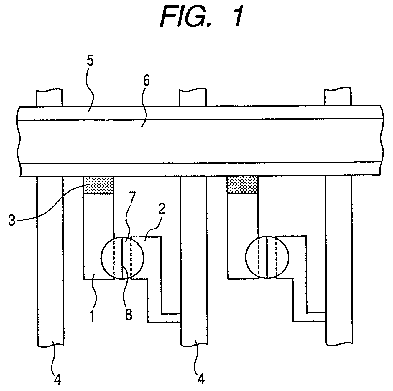
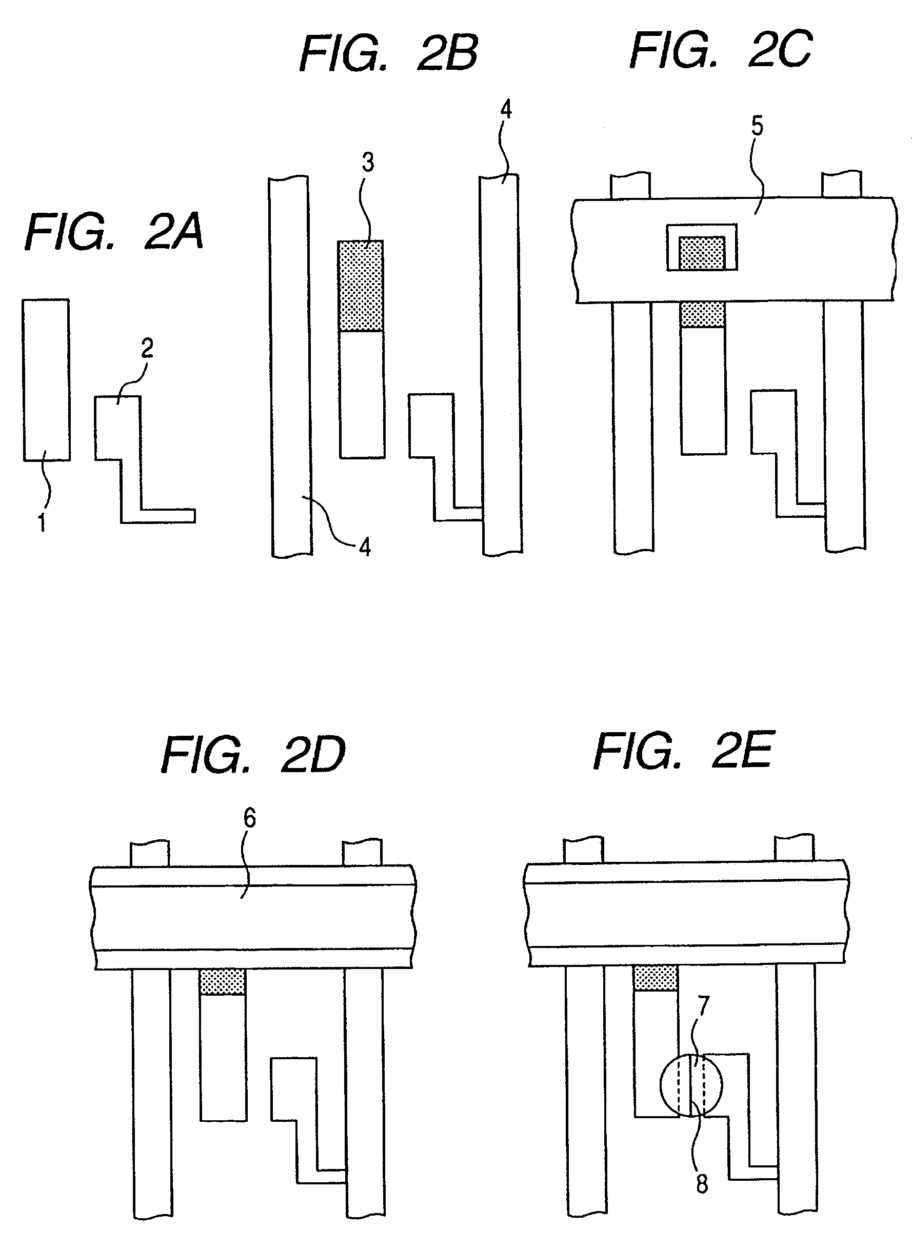
[0115]A rear plate configured as shown in FIG. 1 has been produced in accordance with processes shown in FIGS. 2A to 2E. In the present example, for a substrate, glass with thickness of 2.8 mm of PD-200 (produced by Asahi Glass Co., Ltd.) with few alkali components and moreover SiO2 film with film thickness of 100 nm has been coated to form a sodium block layer on that glass substrate.
Forming of Device Electrode
[0116]Pt film with film thickness of 20 nm was formed with a sputtering method onto the above described glass substrate. Thereafter, photoresist was coated over the whole surface, and subject to patterning with a series of photolithography technology of exposure, development and etching, a scan signal device electrode 1 and an information signal device electrode 2 were formed (FIG. 2A). Electric resistivity of those device electrodes 1 and 2 was 0.25×10⁻⁶ [Ωm]. In addition, the scan signal device electrode 1 was shaped to have width of 30 μm and length of 150 μm.
Forming of In...
example 2
[0151]As shown in FIG. 8, a rear plate was produced to have the same configuration as that in Example 1 except that width of the additional electrode 3 is narrower than that of the scan signal device electrode 1 and the insulating layer 5 covers the information signal wiring 4. Here, as described above, the information signal wiring is covered by the insulating layer 5, and therefore is now shown in FIG. 8.
[0152]The additional electrode 3 of the present example was shaped to have thickness of approximately 5 μm, width of 20 μm and length of 150 μm. In addition, the insulating layer 5 extended on the information signal wiring 4 was shaped to have width of 30 μm. FIG. 9 shows a sectional view cut along 9-9 in FIG. 8. Here, in the present example, the information signal wiring 4 is covered by the insulating layer 5, but resistance of the scan signal side to GND is 10 times lower than that of the information signal side to GND so that discharge current flows to the scan signal side, and...
example 3
[0170]As shown in FIG. 11, a display panel was produced as in Example 1 except that a kink portion 51 was formed in the scan signal device electrode 1. The scan signal device electrode 1 of the present example was shaped to have width of 10 μm and length of 80 μm in the portion contacting the device film 7 and width of 30 μm and length of 100 μm in the portion contacting the additional electrode 3. The pixel amount was set to 3072×768 and pixel pitch was set to 200×600 μm.
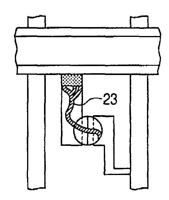
[0171]As prior consideration, current with waveform of a triangular wave was applied (a probe was brought into contact with the scan signal wiring 6 and the device film 7) to the scan signal device electrode 1 in the present Embodiment 3 and the scan signal device electrode 1 in the present Embodiment 1 to, confirm device electrode damage. As a result thereof, the cathode spot in the scan signal device electrode 1 in Example 1 moved to the additional electrode 3 at approximately 300 mA while the cathode spot in the...
PUM
 Abstract
Description
Claims
Application Information
 - R&D
- Intellectual Property
- Life Sciences
- Materials
- Tech Scout
- Unparalleled Data Quality
- Higher Quality Content
- 60% Fewer Hallucinations
Browse by: Latest US Patents, China's latest patents, Technical Efficacy Thesaurus, Application Domain, Technology Topic, Popular Technical Reports.
© 2025 PatSnap. All rights reserved.Legal|Privacy policy|Modern Slavery Act Transparency Statement|Sitemap|About US| Contact US: help@patsnap.com


