
Fixed-pixel display device and cold cathode field electron emission display device

a display device and display device technology, applied in the direction of instruments, static indicating devices, etc., can solve the problems of difficult to smoothly display the image, the leading edge and trailing edge waveforms of voltage v/sub>data/sub>to be applied to the data electrodes are still difficult to become steep, and the response for the display of images is reduced. , to achieve the effect of improving the response for the display of images, smooth display of images, and reducing the power consumption of power consumption

Inactive Publication Date: 2008-07-29
SONY CORP
View PDF12 Cites 1 Cited by
  • Summary
  • Abstract
  • Description
  • Claims
  • Application Information

AI Technical Summary

Benefits of technology

[0102]As a particularly preferred material of the electron-emitting portions in the flattened field emission devices, carbon, more specifically diamond, graphite, graphite nanofibers, a carbon nanotube structure, ZnO whiskers, Mgo whiskers, SnO2 whiskers, MnO whiskers, Y2O3 whiskers, NiO whiskers, ITO whiskers, In2O3 whiskers, or Al2O3 whiskers can be mentioned. When the electron-emitting portions are made of such a material, an emitted electron current density required for the cold cathode field electron emission display device can be obtained at a field strength of 5×10⁷ V / m or lower. Diamond is an electrically resistant material and, therefore, can equalize emitted electron currents to be obtained from the respective electron-emitting portions, thereby making it possible to reduce variations in luminance when such flattened field emission devices are incorporated in the cold cathode field electron emission display device. These materials have extremely high durability against sputtering action by ions of residual gas in the cold cathode field electron emission display device and, therefore, can provide the field emission devices with a longer service life.
[0114]Between the cathode electrodes and the electron-emitting portions, a resistive material layer may be arranged. When the surfaces of the cathode electrodes serve as the electron-emitting portions, the cathode electrodes may be formed as a three-layer structure consisting of a conductive material layer, a resistive material layer, and an electron-emitting layer corresponding to the electron-emitting portions. The arrangement of the resistive material layer makes it possible to stabilize the operation of the electron-emitting devices and also to equalize their electron emission characteristics. Examples of the material that makes up the resistive material layer can include carbon-based materials such as silicon carbide (SiC) and SiCN, semiconductor materials such as SiN and amorphous silicon, and high-melting metal oxides such as ruthenium oxide (RuO2), tantalum oxide and tantalum nitride. As a formation process of the resistive material layer, sputtering, CVD or screen printing can be mentioned, for example. Its resistivity can be set generally at 1×10⁵ to 1×10⁷Ω, preferably at several MΩ.
[0117]The banks have a function to prevent electrons, which are recoiled from the phosphor regions, or secondary electrons, which are emitted from the phosphor regions, from entering other phosphor regions and causing a so-called optical crosstalk (color turbidity). When electrons, recoiled from the phosphor regions or emitted from the phosphor regions, have flown toward other phosphor regions, the banks also have a function to prevent these electrons from impinging on the other phosphor regions.
[0122]As the phosphor material which forms the luminescent crystalline particles, a suitable phosphor material can be selected from conventionally-known phosphor materials and can be used. In the case of displaying in colors, it is preferred to combine phosphor materials which have color purities close to the primaries specified by the NTSC, can achieve a white balance when the primaries are mixed, are short in persistence time, and have primaries having substantially the same persistence time. Examples of the phosphor material which forms the red-color-emitting phosphor regions can include (Y2O3:Eu), (Y2O2S:Eu), (Y3Al5O12:Eu), (YBO3:Eu), (YVO4:Eu), (Y2SiO5:Eu), (Y0.96P0.60V0.40O4:Eu0.04) [(Y,Gd)BO3:Eu], (GdBO3:Eu), (ScBO3:Eu), (3.5MgO.0.5MgF2.GeO2:Mn), (Zn3(PO4)2:Mn), (LuBO3:Eu), and (SnO2:Eu). Examples of the phosphor material which forms the green-color-emitting phosphor regions can include (ZnSiO2:Mn), (BaAl12O19:Mn), (BaMg2Al16O27:Mn), (MgGa2O4:Mn) (YBO3:Tb), (LuBO3:Tb), (Sr4Si3O8Cl4:Eu), (ZnS:Cu,Al), (ZnS:Cu,Au,Al) (ZnBaO4:Mn), (GbBO3:Tb), (Sr6SiO3Cl3:Eu) (BaMgAl14O23:Mn), (ScBO3:Tb), (Zn2SiO4:Mn), (ZnO:Zn), (Gd2O2S:Tb), and (ZnGa2O4:Mn). Examples of the phosphor material which forms the blue-color-emitting phosphor regions can include (Y2SiO5:Ce), (CaWO4:Pb), CaWO4, YP0.85V0.15O4, (BaMgAl14O23:Eu), (Sr2P2O7:Eu), (Sr2P2O7:Sn) (ZnS:Ag,Al), (ZnS:Ag), ZnMgO, and ZnGaO4.
[0129]In the present invention, (1) when the input value is not smaller than the first reference value, the first switching circuit is maintained in an ON state for a predetermined duration shorter than the fixed duration on a basis of the output from the comparator, and during the predetermined duration, a first voltage V1 is applied to the data electrode in the nth column (or, the nth cathode electrode or gate electrode); and (2) when the input value is not greater than the second reference value, the second switching circuit is maintained in an ON state for a predetermined duration shorter than the fixed duration on a basis of the output from the comparator, and during the predetermined duration, a second voltage V2 is applied to the data electrode in the nth column (or, the nth cathode electrode or gate electrode). Described specifically, when the difference between the value of data for controlling the state of light emission at each light-emitting region constituted by a scanning electrode or the value of data for controlling the state of light emission at each of a multiple number N of electron-emitting regions constituted by a gate electrode and cathode electrode and the value of data preceding the above-mentioned value by one sequence is not smaller than the first reference value or not greater than the second reference value, the actuation driver operates and functions as a kind of compensation circuit that compensates for the leading-edge and trailing-edge waveforms of a voltage to be applied to the electrode. Accordingly, the leading-edge and trailing-edge waveforms of the voltage to be applied to the electrode can be made steep. As a result, it is possible to improve the response for the display of an image and hence, to achieve a smooth display of the image. Moreover, an increase in power to be consumed in the fixed pixel display device or cold cathode field electron emission display device can be reduced because the duration (time) during which the first voltage V1 or the second voltage V2 is applied to the data electrode in the nth column (or the nth cathode electrode or gate electrode) is shorter than the fixed duration. In addition, an image with its contour emphasized can be obtained, thereby bringing about a still further merit that an increased degree of sharpness is available on an image to be visualized.

Problems solved by technology

Unless the waveform of the voltage VDATA to be applied to the data electrode is steep, the response for the display of an image is reduced, thereby making it difficult to smoothly display the image.
In a cold cathode field electron emission display device, large capacitance components generally tend to exist in data electrodes, for example, cathode electrodes, and as a consequence, the leading-edge and trailing-edge waveforms of voltages VDATA to be applied to the data electrodes are still more difficult to become steep.

Method used


Image

  • Fixed-pixel display device and cold cathode field electron emission display device
  • Fixed-pixel display device and cold cathode field electron emission display device
  • Fixed-pixel display device and cold cathode field electron emission display device

Examples


example 1

[0145]Example 1 relates to a fixed pixel display device, according to the present invention, and also to a cold cathode field electron emission display device, according to a first embodiment of the present invention.

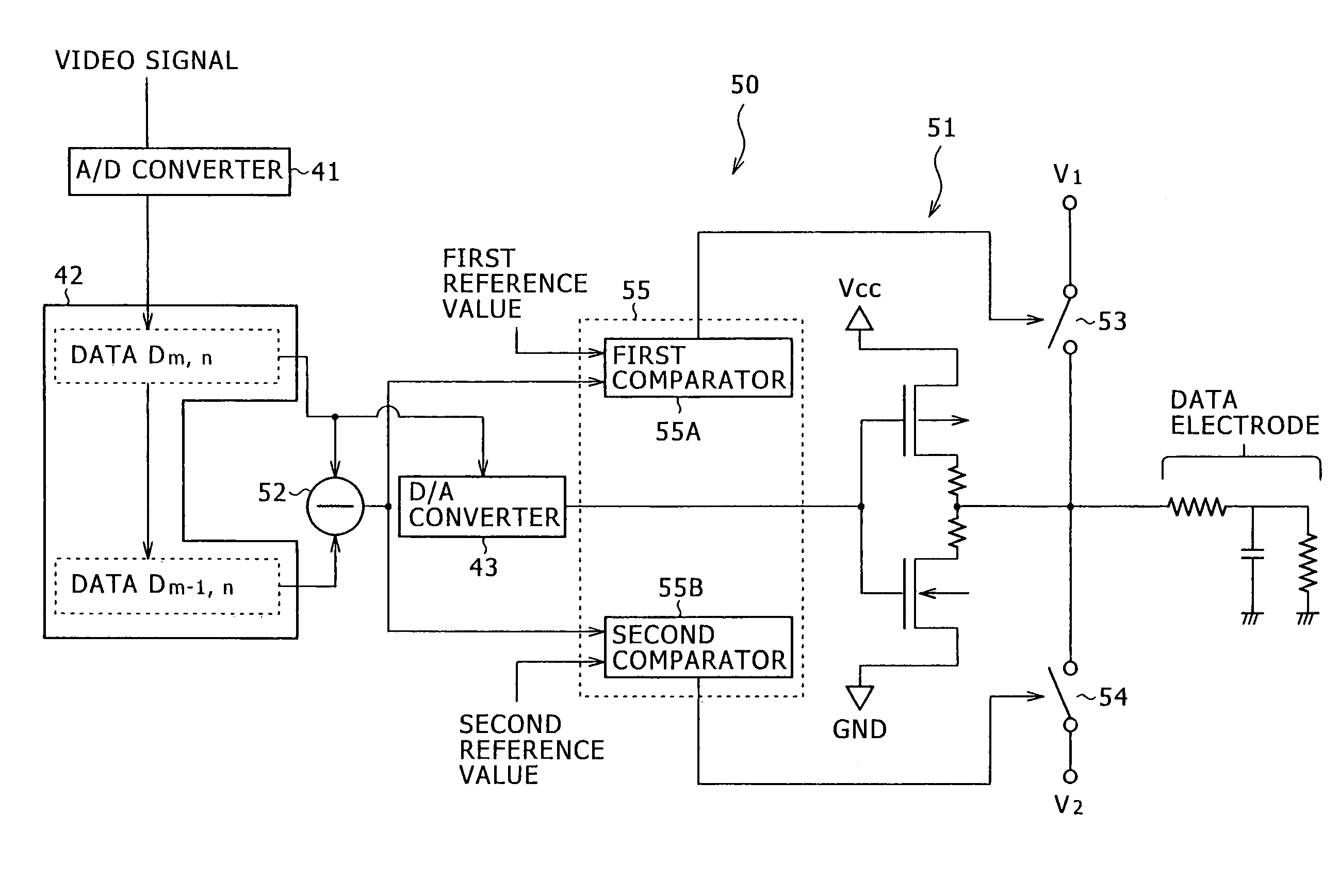
[0146]A circuit diagram of an actuation driver and the like in Example 1 is shown in FIG. 1, a conceptual diagram of the fixed pixel display device of Example 1 is illustrated FIG. 2, and the state of application of a voltage on a data electrode (cathode electrode) in the fixed pixel display device or cold cathode field electron emission display device (which may hereinafter be collectively called simply “display”) of Example 1 is schematically depicted in FIG. 3. Further, a schematic fragmentary end view of the cold cathode field electron emission display device of Example 1 is shown in FIG. 5, an exploded, schematic fragmentary perspective view of a cathode panel CP and anode panel AP is illustrated in FIG. 6, and as schematic fragmentary plan views, layouts of phosph...

example 2

[0196]Example 2 relates to a fixed pixel display device, according to the present invention, and also to a cold cathode field electron emission display device, according to a second embodiment of the present invention.

[0197]A circuit diagram of an actuation driver and the like in Example 2 and a conceptual diagram of the fixed pixel display device of Example 2 are similar to those shown in FIG. 1 and FIG. 2, respectively, and a schematic fragmentary end view of the cold cathode field electron emission display device of Example 2, an exploded, schematic fragmentary perspective view of a cathode panel CP and anode panel AP, and layouts of phosphor regions and the like are similar to those depicted in FIG. 5, FIG. 6, and FIG. 7 through FIG. 10. The state of application of a voltage to data electrodes (gate electrodes) in the display of Example 2 is schematically illustrated in FIG. 4.

[0198]The cold cathode field electron emission display device of Example 2 is constructed of the cathod...


PUM


Abstract

A fixed pixel display device has a construction such that the leading-edge and trailing-edge waveforms of a voltage to be applied to a data electrode can be made steep. The fixed pixel display device is provided with scanning electrodes, data electrodes connected to actuation drivers (50), and light-emitting regions. Each of the actuation drivers (50), includes a switching circuit, an output circuit (51), and a subtraction circuit (52). The switching circuit is equipped with a first switching circuit (53), a second switching circuit (54), and a comparator (55). When a difference (Dm,n-Dm−1,n) between values of data for controlling states of light emission at light-emitting regions, composed by the scanning electrodes in mth and (m−1)th rows, is not smaller than a first reference value [not greater than a second reference value], the first switching circuit (53) [the second switching circuit (54)] is maintained in an ON state to apply a first voltage V1 [a second voltage V2] to the data electrode in an nth column. When the difference is smaller than the first reference value and is greater than the second reference value, the first and second switching circuits, (53) and (54), are maintained in OFF states, respectively.

Description

TECHNICAL FIELD[0001]This invention relates to a fixed pixel display device and also to a cold cathode field electron emission display device.BACKGROUND ART[0002]As fixed pixel display devices, each having a structure that a multiple number (M) of stripe-shaped scanning electrodes extending in a first direction and another multiple number N of stripe-shaped data electrodes extending in a second direction different from the first direction (for example, intersecting at right angles with), are provided and light-emitting regions, formed of overlap regions of the scanning electrodes and the data electrodes, are arrayed in a two-dimensional matrix form of M rows×N columns, known examples include cold cathode field electron emission display devices, liquid crystal displays, organic electroluminescence displays, and inorganic electroluminescence displays (see, for example, Japanese Patent Laid-open No. Hei 11-296131). In these fixed pixel display devices, the line-sequential drive method ...

Claims


Application Information

Patent Timeline
Patent Type & Authority Patents(United States)
IPC IPC(8): G09G3/22G09G3/20
CPCG09G3/22G09G2310/027
Inventor IKEDA, HIROYUKI
Owner SONY CORP
Learn More