Photoelectron spectroscopy apparatus and method of use

a technology of photoelectron spectroscopy and apparatus, applied in the direction of optical radiation measurement, semiconductor/solid-state device testing/measurement, instruments, etc., can solve the problems of inability to view a particular pad, contaminating the inside of the tool, and unsatisfactory images, etc., to increase the collection efficiency of the monochromator

Active Publication Date: 2008-07-15
NOVA MEASURING INSTRUMENTS INC +1
View PDF7 Cites 3 Cited by
  • Summary
  • Abstract
  • Description
  • Claims
  • Application Information

AI Technical Summary

Benefits of technology

[0019]In an embodiment of the present invention the electromagnetic radiation source includes an electron source for providing an electron beam for irradiating an anode with electrons to produce electromagnetic radiation, such as X-rays, and a monochromator to focus the emitted electromagnetic radiation onto the substrate or specimen. In embodiments of the present invention, the electron source includes shaping means, such as an octopole or aperture shutters to shape the electron beam into a desired shape or profile. The electron beam can be shaped into a desired profile, such as but not limited to a circle, an elongated oval, a square, and a rectangle. In an embodiment of the present invention, an electron beam is shaped into an elongated oval or rectangle having a length is 1-3 times larger than its width. Additionally, in an embodiment of the present invention, a large area monochromator with a large solid angle is utilized to increase the collection efficiency of the monochromator. A large area monochromator with a large solid angle enables the e-beam shape to be transferred into an X-ray profile pattern which is highly correlated to the e-beam shape on the anode.

Problems solved by technology

However, typically the vision systems are only able to view the pads at an angle, so the image is not ideal.
Additionally, the systems are not able to view a particular pad while it is being tested.
Furthermore, the vision systems typically include multiple actuators and other moving parts, which create contaminates within the tool.
The separate stage occupies a considerable amount of space within the tool, and the magnetic lenses must be located below the stage, which detrimentally affects the effectiveness of the magnetic lens.
If the magnetic lens requires any sort of maintenance, the vacuum must be broken, which increases the likelihood that the interior of the tool will be contaminated.

Method used


Image

  • Photoelectron spectroscopy apparatus and method of use
  • Photoelectron spectroscopy apparatus and method of use
  • Photoelectron spectroscopy apparatus and method of use

Examples


Embodiment Construction

[0038]In the following description, various aspects of the present invention will be described, and various details set forth in order to provide a thorough understanding of the present invention. However, it will be apparent to those skilled in the art that the present invention may be practiced with only some or all of the aspects of the present invention, and the present invention may be practiced without the specific details. In other instances, well-known features are omitted or simplified in order not to obscure the present invention.

[0039]It should be understood the FIGS. 1A through 10C are merely illustrative and may not be drawn to scale.

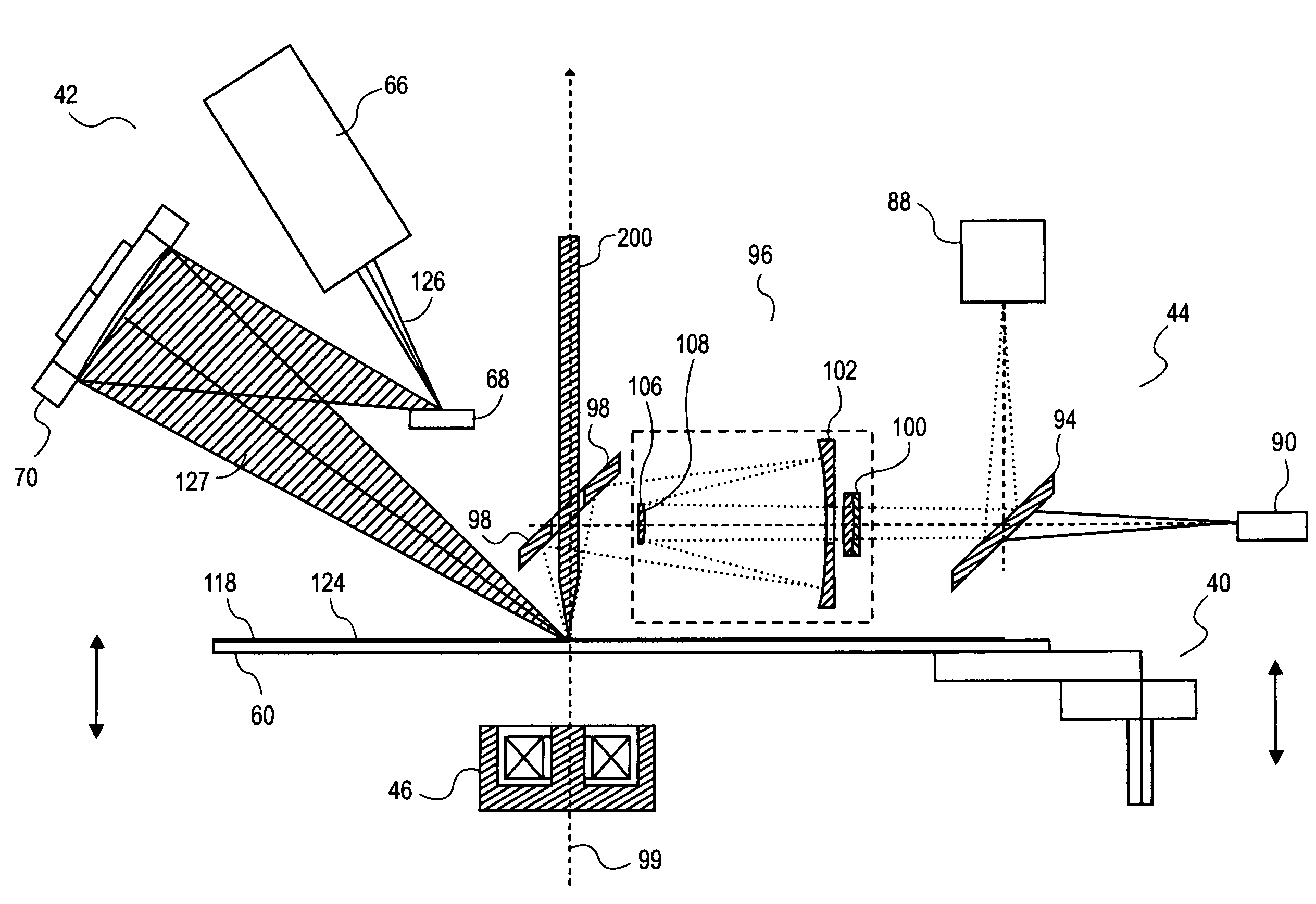
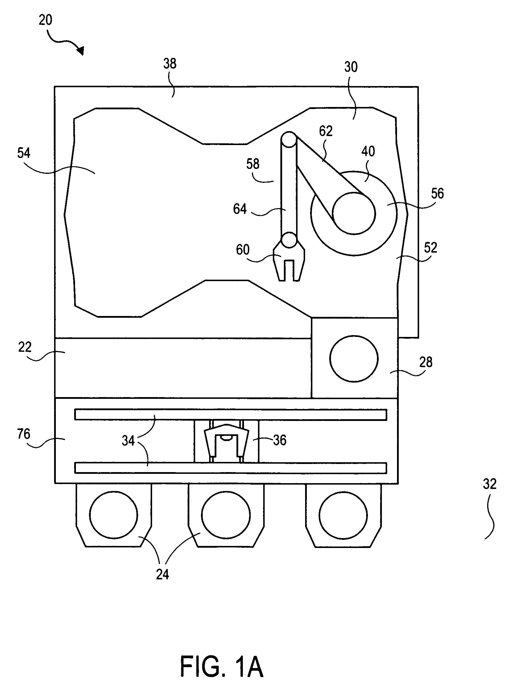
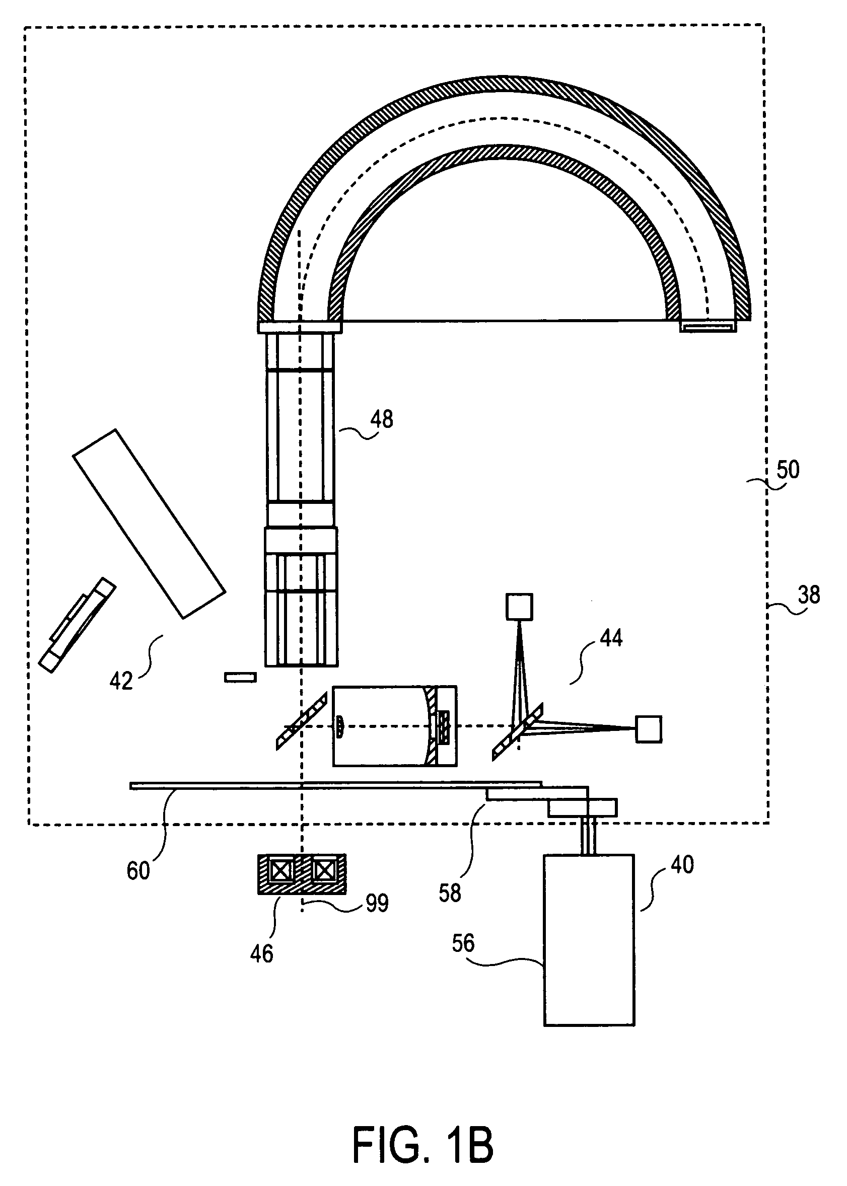
[0040]An embodiment of the present invention provides what is known in the art as a “metrology tool.” The metrology tool may include load-lock chamber and a metrology chamber, enclosing a vacuum chamber, with a loading portion and a testing portion. A robotic stage may be located within loading portion of the metrology chamber to transport ...


PUM


Abstract

According to one aspect of the present invention, a substrate processing system is provided. The system may include a chamber wall enclosing a chamber, a substrate support positioned within the chamber to support a substrate, an electromagnetic radiation source to emit electromagnetic radiation onto the substrate on the substrate support, the electromagnetic radiation causing photoelectrons to be emitted from a material on the substrate, an analyzer to capture the photoelectrons emitted from the substrate, and a magnetic field generator to generate a magnetic field within the chamber and guide the photoelectrons from the substrate to the analyzer.

Description

BACKGROUND OF THE INVENTION[0001]1). Field of the Invention[0002]The present invention relates to a method, apparatus, and system for processing semiconductor substrates, particularly to a metrology tool for use in processing semiconductor substrates.[0003]2). Discussion of Related Art[0004]Integrated circuits are formed on semiconductor substrates such as wafers. The formation of the integrated circuits may include numerous processing steps such as deposition of various layers, etching some of the layers, and multiple bakes. The integrated circuits are then separated into individual microelectronic dice, which are packaged and attached to circuit boards.[0005]During the various processing steps involved in the creation of the integrated circuits, various layers of different materials, such as conductors, dielectrics, and semiconductor, are formed on the surface of the wafer where the integrated circuits are being formed. The manufacturers of the integrated circuits often test the c...

Claims


Application Information

Patent Timeline
Patent Type & Authority Patents(United States)
IPC IPC(8): H01J40/00
CPCG01N23/2273G01N2223/6116H01J2235/08G01N2223/085G01J3/42H01L22/00
Inventor SCHUELER, BRUNO W.REED, DAVID A.
Owner NOVA MEASURING INSTRUMENTS INC
Why Eureka
Try Eureka