Solid state image sensing apparatus with enhanced sensitivity realized by improving linear characteristic of photodiode and its driving method

a photodiode and linear characteristic technology, applied in the field of solid-state image sensing apparatuses, can solve the problems of limited bias modulation amount and no increase in saturation signal charge qs, and achieve the effect of improving linear characteristic of photodiodes and enhancing sensitivity

Inactive Publication Date: 2008-04-29
PANASONIC CORP
View PDF15 Cites 4 Cited by
  • Summary
  • Abstract
  • Description
  • Claims
  • Application Information

AI Technical Summary

Benefits of technology

[0025]An object of the present invention is to provide a solid state image sensing apparatus with enhanced sensitivity realized by improving linear characteristic of photodiode and its driving method.

Problems solved by technology

Thus, the amount of the bias modulation is limited.
However, no increase in the amount of saturation signal charge Qs is observed because the overflow barrier (OFG) at charge storage time is not made higher.

Method used


Image

  • Solid state image sensing apparatus with enhanced sensitivity realized by improving linear characteristic of photodiode and its driving method
  • Solid state image sensing apparatus with enhanced sensitivity realized by improving linear characteristic of photodiode and its driving method
  • Solid state image sensing apparatus with enhanced sensitivity realized by improving linear characteristic of photodiode and its driving method

Examples


first embodiment

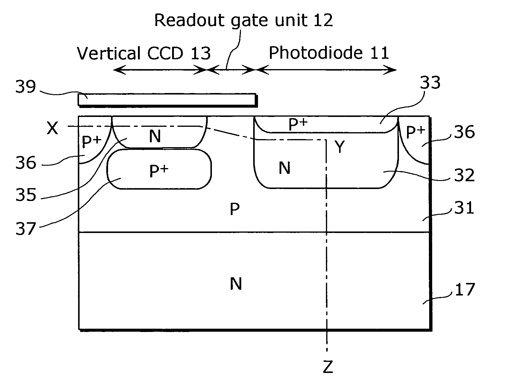
[0069]The solid state image sensing apparatus in the present invention is characteristic in that it intentionally makes the height of the overflow barrier (OFB) higher than the readout gate barrier (refer to FIG. 12A) at the starting time of the exposure period (refer to T3 and T4 in FIG. 7) and in that it temporally lowers the height of the overflow barrier (OFB) so as to sweep out excessive charge on the substrate (refer to FIGS. 13 and 14) during the time period from the end of the exposure period to the start of sweeping out the vertical CCDs (refer to T5 in FIG. 7). In this way, it improves the linear property in photodiodes and enhances the sensitivity.

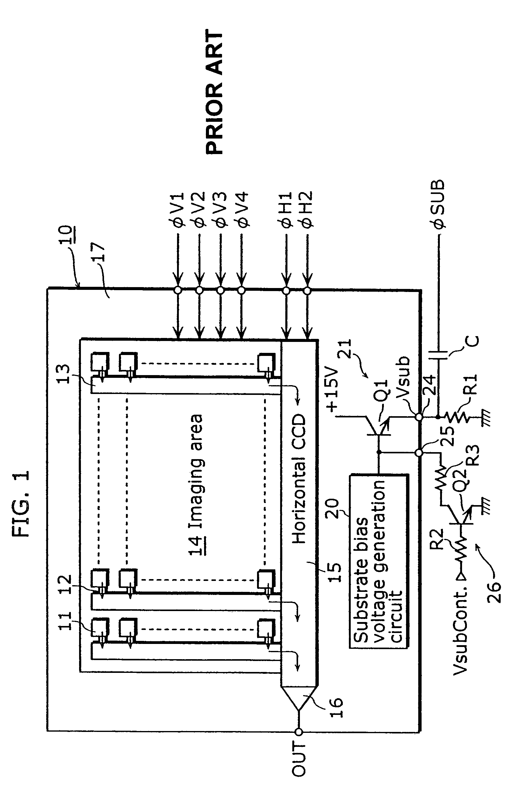
[0070]FIG. 4 is a block diagram showing the outline structure of the solid state image sensing apparatus 1 in the first embodiment of the present invention. The solid state image sensing apparatus 1 comprises a lens 2, a mechanical shutter 3, a driver unit 4, a signal processing unit 5 and a solid state image sensor 10.

[0071]In ...

second embodiment

[0104]Consequently, a desirable timing for a substrate shutter will be explained as to the solid state image sensing apparatus in the second embodiment as the first footnote.

[0105]The above-mentioned second bias voltage is applied immediately after the substrate shutter pulse has been applied to the end of the readout period of the second field in FIG. 7, but it is possible to obtain an effect of improving a linear property even in the case of during or before the application of the substrate shutter pulse. Therefore, applying the second bias voltage during the whole exposure period increases the amount of the saturation signal charge Qs in the exposure period, which enlarges the linear area for determining a constant rate of the amount of the saturation signal charge Qs.

[0106]Further, desirably, the first bias voltage should be switched to the second bias voltage immediately after the substrate shutter pulse has been applied. Therefore, as the substrate shutter pulse is applied und...


PUM


Abstract

A driver unit of a solid state image sensing apparatus changes the substrate bias voltage from a first bias voltage to a second bias voltage which is lower than the first bias voltage and is for making a height of an overflow barrier higher than a height of the barrier in the readout gate. Moreover, the driver unit lowers the height of the overflow barrier by superimposing a saturation signal control pulse on the second bias voltage after an end of an exposure period and before sweeping out all the signal charge of vertical CCDs.

Description

BACKGROUND OF THE INVENTION[0001](1) Field of the Invention[0002]The present invention relates to a solid state image sensing apparatus with a Charge Coupled Device (CCD) that has an overflow drain (OFD) structure and its driving method.[0003](2) Description of the Related Art[0004]Recently, electric devices for recording images such as digital cameras, digital video cameras and cellular phones with a camera have become popular, and image sensors such as CCD image sensors have been refined as resolution becomes higher.[0005]FIG. 1 is a block diagram showing the structure of a conventional CCD solid state image sensing apparatus that is disclosed in patent literature and the like. In the figure, the solid state image sensor 10 comprises a plurality of photodiodes 11 that are aligned two-dimensionally, a plurality of readout gate units 12, a plurality of vertical CCDs 13, a horizontal CCD 15, an output amplifier 16, a substrate bias generating circuit 20 and a transistor Q1. The figur...

Claims


Application Information

Patent Timeline
Patent Type & Authority Patents(United States)
IPC IPC(8): H04N5/335H01L27/148H04N5/341H04N5/353H04N5/369H04N5/372
CPCH04N3/1568H04N5/3592H04N5/3728H04N25/622H04N25/73G05F3/205G05F3/24H04N25/766
Inventor KOHNO, AKIYOSHIMUTOH, NOBUHIKOFUJITA, TAKESHI
Owner PANASONIC CORP
Why Eureka
Try Eureka