Device and method for optical center detection

a technology of optical center detection and optical center, which is applied in the direction of optical radiation measurement, instruments, television systems, etc., can solve the problems of not revealing the suitably adjusted position of the sensor array along the direction, the design using the position pin becomes too complicated, and the quality of the outputted digital image is affected, so as to achieve easy determination and simple and more accurate

Inactive Publication Date: 2007-12-11
ASIA OPTICAL CO INC
View PDF1 Cites 19 Cited by
  • Summary
  • Abstract
  • Description
  • Claims
  • Application Information

AI Technical Summary

Benefits of technology

[0011]When light is parallel to the optical axis and is incident to the lens, the distribution of the illumination is axially symmetrical for any plane perpendicular to the optical axis. Thus a planar sensor array perpendicular to the optical axis is used to receive the light transmitted from the lens. When the distribution of the illumination detected on the sensor array is axial symmetrically, the intersection of the optical axis and the sensor array, or the optical center referred to in the present invention, can be inferred as being aligned based on the symmetry. In an embodiment, the distribution of the illumination on the image plane is analyzed and contoured, and the optical center is computed as a geometrical center of the “illumination contour”. Compared with the conventional method for the optical center detection utilizing the focal point, the method disclosed by the present invention is simpler and more accurate. Furthermore, the offset between the optical center and the center of the sensor array can be easily determined.

Problems solved by technology

The mis-alignment of the optical center and the center of the sensor array will affect the quality of the outputted digital image.
However, for the high-end single lens reflex camera, the lens is replaceable, so the design using the position pin becomes too complicated.
However, U.S. Pat. No. 5,483,284 did not disclose how to suitably adjust the position of the sensor array along the direction perpendicular to the optical axis.
However, “optical axis” is intangible, so no practical method has existed yet to determine whether the optical center and the center of the sensor array are aligned.
However, in reality, the noise will make the position of the highest illumination differ from the actual focal point, and hinder the alignment of the optical center and the center of the sensor array.

Method used


Image

  • Device and method for optical center detection
  • Device and method for optical center detection
  • Device and method for optical center detection

Examples


Embodiment Construction

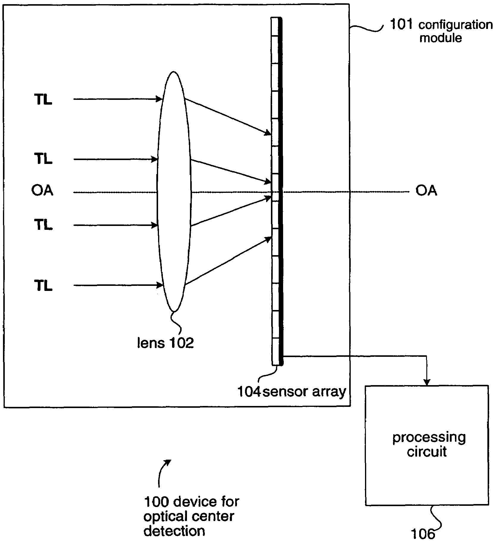
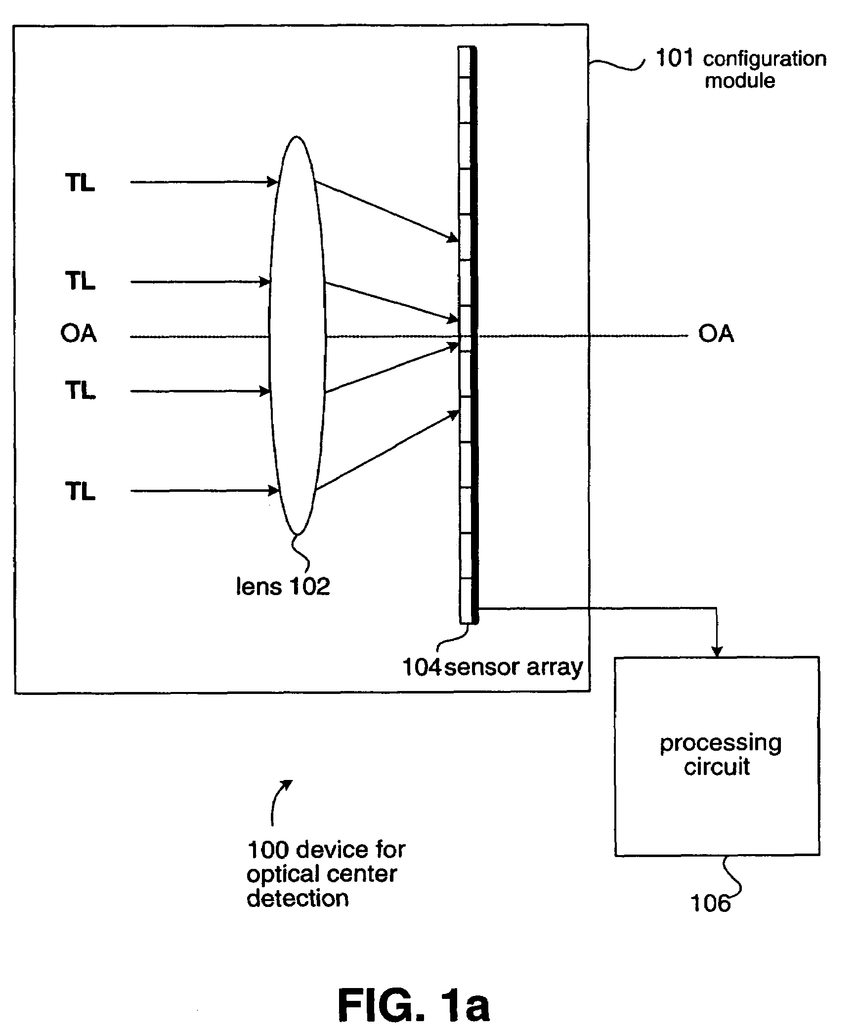
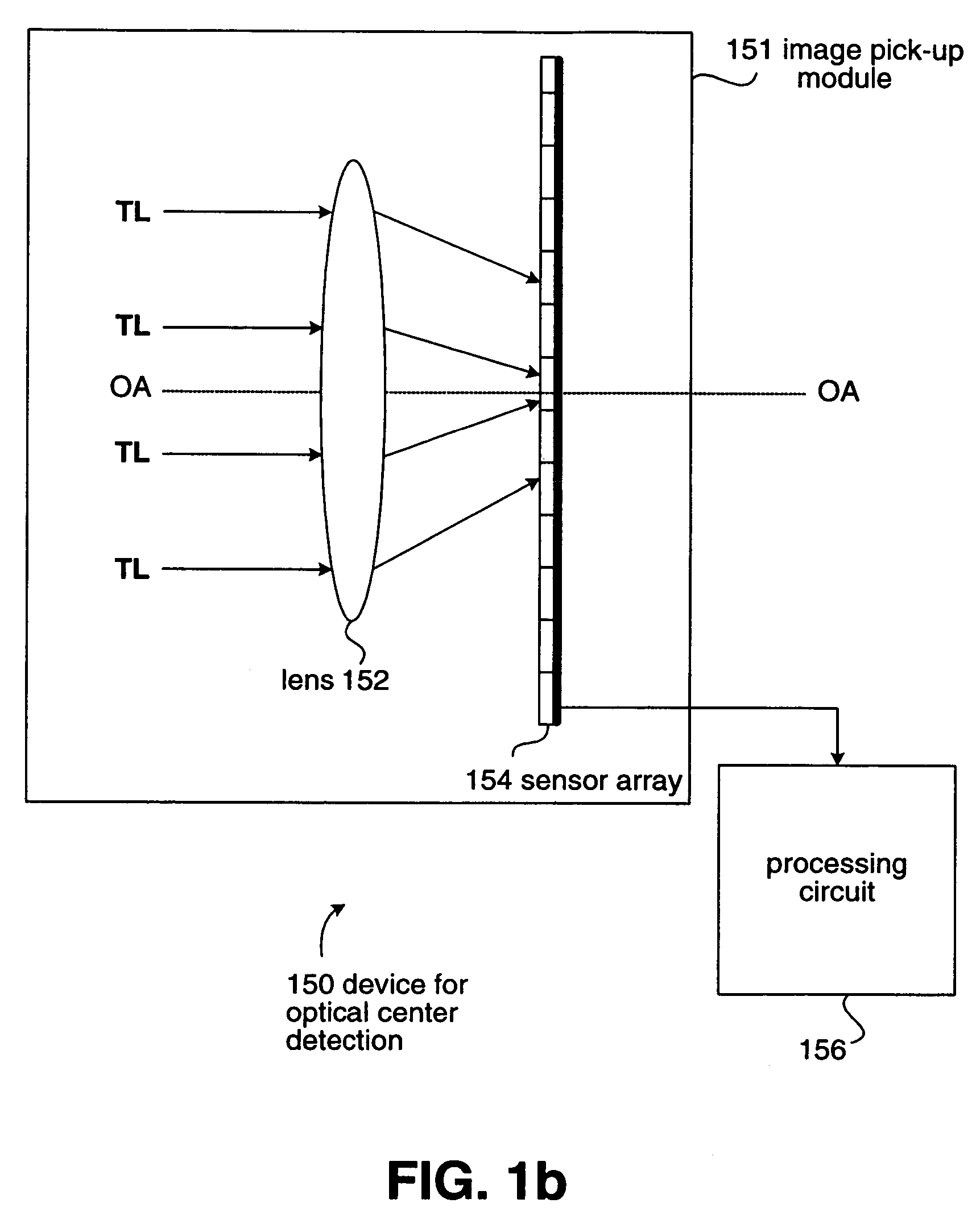
[0022]Referring to FIG. 1a, a device 100 is provided for computing an optical center of a sensor array 104 relative to a lens 102. The device 100 includes a configuration module 101 and a processing circuit 106. Note that the combination of the lens 102 and the sensor array 104 can form an image pick-up module for the device 100 to generate a digital image corresponding to a target.

[0023]In an embodiment, the configuration module 101 has a base (not shown) for positioning the lens 102 and the sensor array 104 thereon, and provides the electrical connection with the sensor array 104. Alternatively, according to the result of computation mentioned hereinafter, the base of the configuration module 101 can be adjusted for the alignment of lens 102 relative to the sensor array 104. After the alignment was done, the relative position of the lens 102 to the sensor array 104 can be fixed using the conventional packaging technology. The packaged lens 102 and the sensor array 104 together can...


PUM

PropertyMeasurementUnit
optical centeraaaaaaaaaa
distanceaaaaaaaaaa
opticalaaaaaaaaaa

Abstract

A device is presented for computing an optical center of a sensor array relative to a lens. The sensor array includes a plurality of sensor units, and each sensor unit has a position on the sensor array. The lens defines an optical axis. The device includes a configuration module and a processing circuit. The configuration module is provided for positioning the lens and the sensor array thereon. When test light is parallel to the optical axis and is incident to the lens, the sensor array receives the test light transmitted by the lens so that each sensor unit outputs a value. The processing circuit is linked to the sensor array for receiving values outputted from the sensor units and selecting positions of sensor units outputting a specific value among the values, for computing the optical center of the sensor array.

Description

CROSS REFERENCE TO RELATED APPLICATIONS[0001]This application claims the right of priority based on Taiwan Patent Application No. 093120225 entitled “Device and Method for Optical Center Detection”, filed on Jul. 6, 2004, which is incorporated herein by reference and assigned to the assignee herein.FIELD OF INVENTION[0002]The present invention relates to a device and a method for optical center detection. More specifically, it relates to a device and a method for optical center detection for a digital image forming system.BACKGROUND OF THE INVENTION[0003]For a digital camera, the lens receives the light and transmits it to the sensor device, such as Charge Coupled Device, CCD. By the CCD, the collected light is transformed into digital image signals which are further stored in the memory. Typically, the sensor device includes a sensor array, conventional types of which include pixels of “320×240”, “640×480”, “1280×960”, “2048×1536”, and so on.[0004]During the assembling process of a...

Claims


Application Information

Patent Timeline
Patent Type & Authority Patents(United States)
IPC IPC(8): G01N21/41G02B27/62H04N5/225
CPCG02B27/62G01J1/0266
Inventor LIN, YI-HSUANLOW, TECK WEE
Owner ASIA OPTICAL CO INC
Why Eureka
Try Eureka