
Distributed balun with a non-unity impedance ratio

a technology of impedance ratio and distribution balun, which is applied in the direction of broad-band transformers, printed inductances, coils, etc., can solve the problems of complex formation of such baluns, and achieve the effect of simple formation

Active Publication Date: 2007-04-03
STMICROELECTRONICS SRL
View PDF5 Cites 18 Cited by
  • Summary
  • Abstract
  • Description
  • Claims
  • Application Information

AI Technical Summary

Benefits of technology

"The present invention provides a solution for a Marchand-type distributed balun with a non-unity impedance ratio. The invention also avoids the need for additional vias and bridges of connection of conductive windings for a balun. The invention is compatible with the forming of a balun by means of superposed conductive windings. The invention includes a mode-switching transformer with coupled lines, in which the lines have different widths to achieve the desired impedance ratio. The widths of the lines are selected according to the impedance ratio desired between the common-mode and differential-mode ports. The transformer includes a first conductive line formed of two primary windings electrically in series, and the length of which is a function of the central operating frequency of the transformer, and a second conductive line formed of two secondary windings electrically in series, with the primary or secondary of the transformer having the smallest impedance having the largest line width. The two windings of each of the conductive lines are superposed in two different metal levels, with the primary or secondary of the transformer having the smallest impedance having the narrowest width. The intertrack between two spirals of a same winding is sized according to the desired impedance."

Problems solved by technology

Further, for impedance ratios other than four or one quarter, the connections of multiple spirals in parallel make the forming of such baluns all the more complex.

Method used


Image

  • Distributed balun with a non-unity impedance ratio
  • Distributed balun with a non-unity impedance ratio
  • Distributed balun with a non-unity impedance ratio

Examples


Embodiment Construction

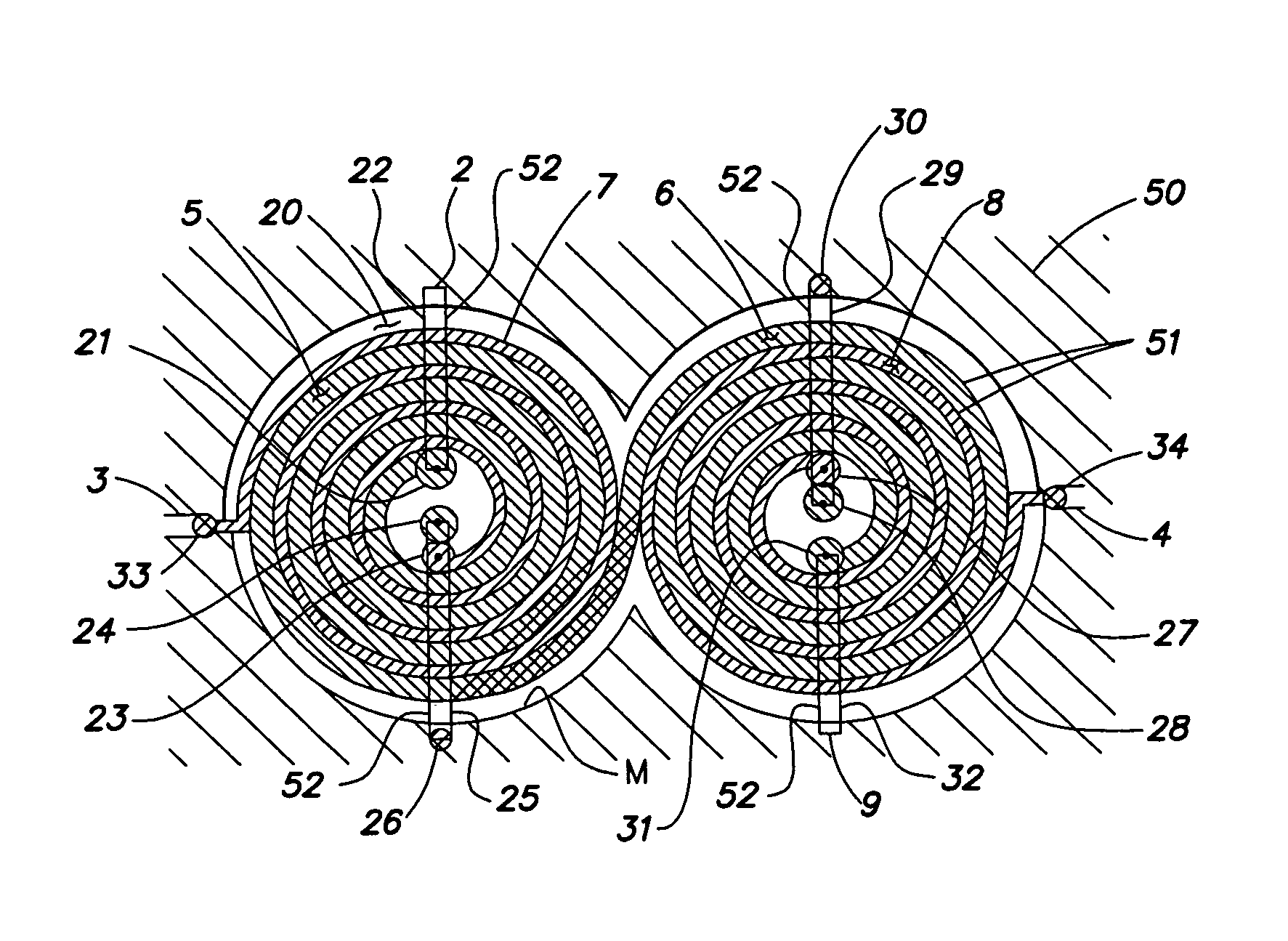
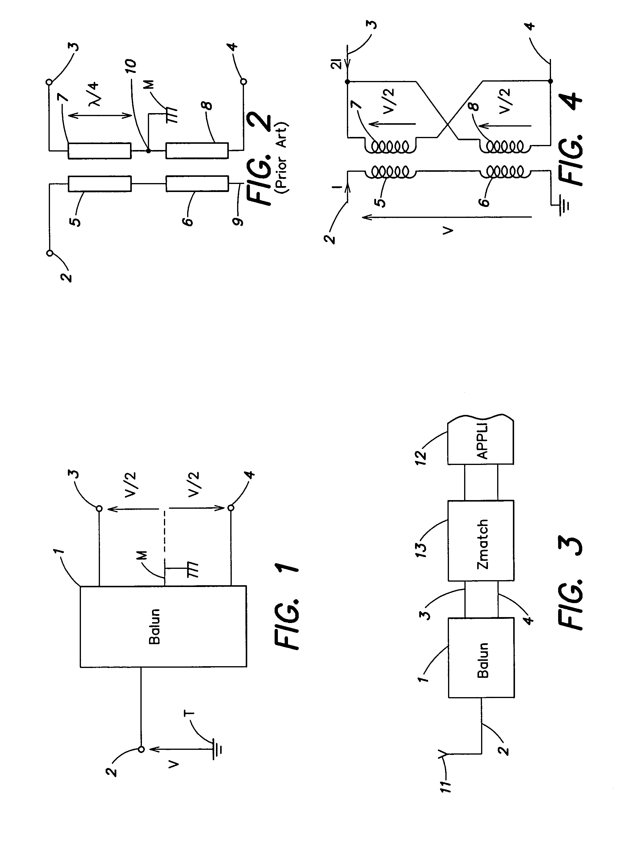
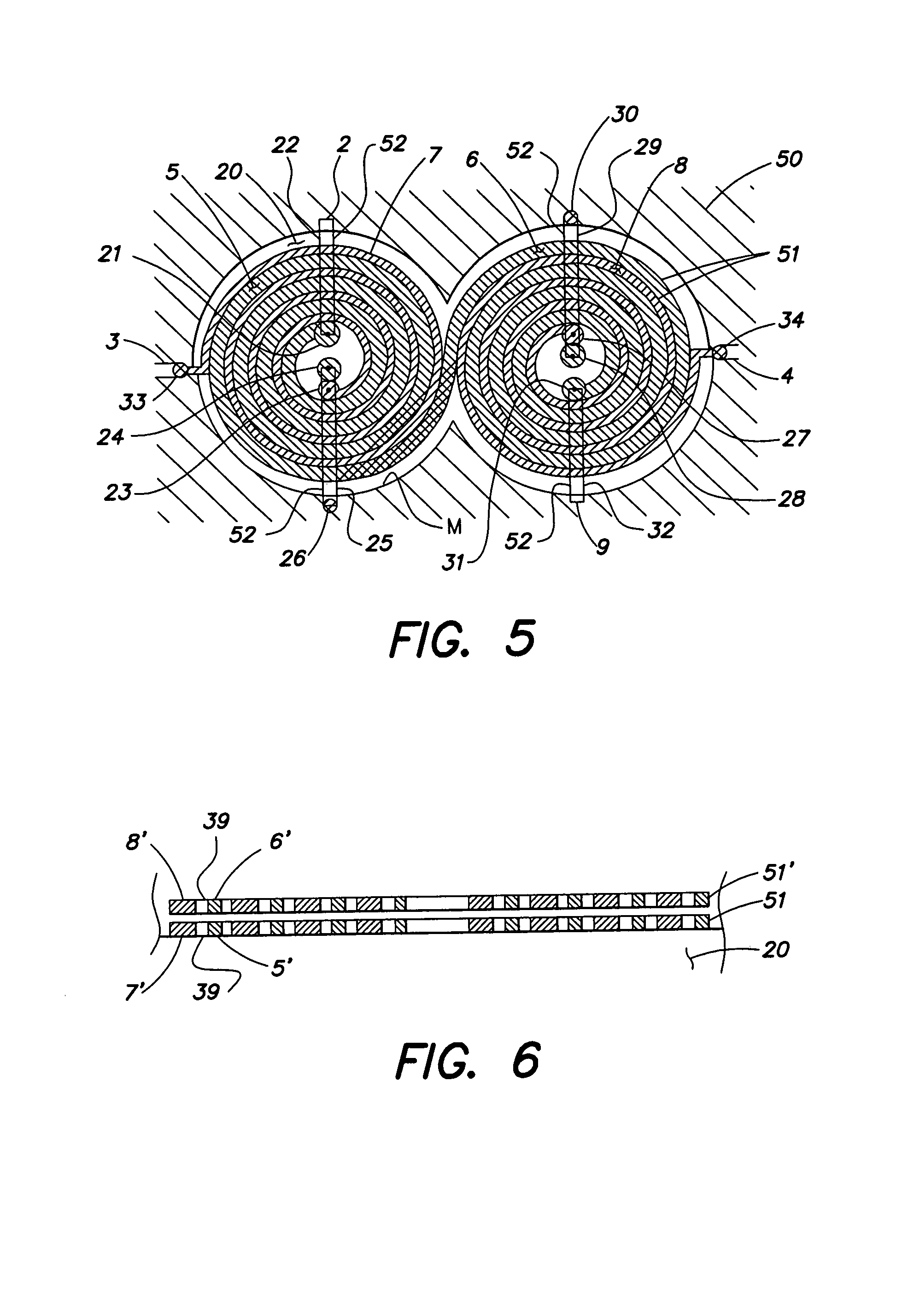
[0026]The same elements have been referred to with the same reference numerals in the different drawings. For clarity, only those elements which are necessary to the understanding of the present invention have been shown in the drawings and will be described hereafter. In particular, the upstream and downstream circuits of a balun have not been described in detail. The present invention applies whatever the circuits or equipment connected on the differential mode side and on the common mode side. Further, the practical forming of conductive windings on a multiple-level substrate has not been described in detail. The present invention may be implemented using conventional techniques of balun forming by means of conductive tracks.

[0027]A feature of the present invention is to provide conductive tracks having different widths between the primary (common mode) and the secondary (differential mode).

[0028]It could have been thought to modify the impedance ratio by modifying the number of ...


PUM

PropertyMeasurementUnit
impedanceaaaaaaaaaa
lengthaaaaaaaaaa
impedance ratioaaaaaaaaaa

Abstract

A mode-switching transformer having a first conductive line formed of two primary windings electrically in series, and the length of which is a function of a central operating frequency of the transformer; and a second conductive line formed of two secondary windings electrically in series, coupled two-by-two with the primary windings, the length of which is a function of said central frequency. The conductive lines exhibit different widths selected according to the desired impedance ratio of the transformer.

Description

BACKGROUND OF THE INVENTION[0001]1. Field of the Invention[0002]The present invention relates to mode-switching transformers which are used to convert a voltage from the common mode to a differential mode and conversely. Such transformers are generally called “balun” (balanced-unbalanced) transformers.[0003]2. Discussion of the Related Art[0004]A mode-switching transformer is, for example, used in radio frequency transceiver chains, for example, of mobile phones. This type of application currently uses devices of balun type, the antenna side being most often associated with a single-ended device.[0005]Two categories of mode-switching transformers are coupled-line or distributed baluns, and baluns with discrete components. Baluns with coupled lines are formed of pairs of coupled conductive tracks, the transformer's operating frequency being conditioned by the line length. Baluns with discrete components are formed of capacitive and inductive components forming LC cells.[0006]The pres...

Claims


Application Information

Patent Timeline
Patent Type & Authority Patents(United States)
IPC IPC(8): H03H7/00H01F5/00H01F17/00H01F19/06H01P5/10H03H7/42
CPCH01F5/003H01P5/10H03H7/42H01F17/0006H01F17/0013H01F19/06H01F2017/0093
Inventor EZZEDDINE, HILAL
Owner STMICROELECTRONICS SRL
Learn More