
Method for customizing an integrated circuit element

a technology of integrated circuits and elements, applied in the field of customizing integrated circuit elements, can solve the problems of difficult to locate the exact point of the circuit on a real circuit, difficulty in locating the exact point of the circuit, and difficulty in achieving the effect of increasing the diversity of the circuits

Inactive Publication Date: 2007-03-13
CENT NAT DETUD SPATIALES C N E S
View PDF6 Cites 20 Cited by
  • Summary
  • Abstract
  • Description
  • Claims
  • Application Information

AI Technical Summary

Benefits of technology

[0016]prior to step b) of defining a composite of logic operators, the method comprises a step of classifying the vectors so as to increase their diversity.

Problems solved by technology

Nevertheless, it is difficult on a real circuit to locate the exact point of the circuit where a measurement is to be performed.
This task is made even more difficult in numerous cases, for example with programmable circuits, because the exact configuration of the real circuit is not known.
In addition, the tracks of the circuit are often smaller in size than the positioning error of the tool used for observing the circuit.

Method used


Image

  • Method for customizing an integrated circuit element
  • Method for customizing an integrated circuit element
  • Method for customizing an integrated circuit element

Examples


Embodiment Construction

[0031]The method of the invention makes it possible to find the exact position of a circuit element on an existing integrated circuit, for example a track, even though the exact layout of the integrated circuit is not known.

[0032]In order to implement the algorithm, it is necessary to know the electrical circuit diagram of the integrated circuit, or at least the logic states of the various tracks of the circuit as a function of a sequence of predetermined tests input to the circuit.

[0033]A defective element is located on an image of the circuit or of a portion of the circuit. The image is processed to show up only the looked-for element, picking it out relative to the other elements which appear normally on the image of the circuit. With the looked-for element picked out in this way in an image of the circuit, it is possible using the coordinates of the element on the image to find the position of said element on the integrated circuit proper and thus to apply a measuring device exa...


PUM


Abstract

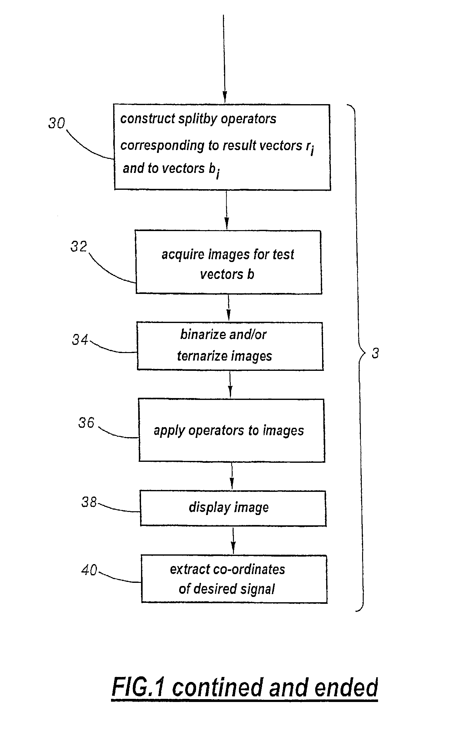
A customizing method includes steps which consist in: a) determining on the basis of a circuit model, a set of vectors each corresponding to a theoretical operating time of the circuit when a predetermined sequence of tests is applied, the coefficients of each vector representing the state of a common set of elements of the circuit among which the element to be customized (12); b) defining on the basis of a comparison of vectors, a composite of logic operators applied on the vectors and enabling to extract the coefficient corresponding to the element to be customized (30); c) producing images of the operating circuit at times corresponding to the vectors whereon is applied the composite of logic operators (32); and d) graphically combining the images produced in accordance with a composite of graphic operators corresponding to the composite of logic operators (36).

Description

FIELD OF THE INVENTION[0001]The present invention relates to a method of picking out an individual integrated circuit element.BACKGROUND OF THE INVENTION[0002]In order to analyze an integrated circuit formed on a semiconductor substrate, it is necessary to perform optical analyses of the circuit in operation, for example by light-emission microscopy or using a scanning electron microscope.[0003]Nevertheless, it is difficult on a real circuit to locate the exact point of the circuit where a measurement is to be performed. This task is made even more difficult in numerous cases, for example with programmable circuits, because the exact configuration of the real circuit is not known. Thus, the real coordinates of the tracks of the circuit are not available. In addition, the tracks of the circuit are often smaller in size than the positioning error of the tool used for observing the circuit.[0004]In contrast, the circuit diagram of the circuit is generally available, even if the real la...

Claims


Application Information

Patent Timeline
IPC IPC(8): G06K9/00G01R31/28G01R31/303G01R31/307G01R31/317
CPCG01R31/2846G01R31/303G01R31/31703G01R31/307
Inventor DESPLATS, ROMAINPERDU, PHILIPPE
Owner CENT NAT DETUD SPATIALES C N E S
Learn More