
Analog to digital converter using both analog and digital offset voltages as feedback

a digital and analog converter technology, applied in the field of analog-to-digital (a/d) conversion units, can solve the problems of residual offset voltage, linearity error vofs-ad of the a/d conversion unit disclosed in the cited patent application, and add to the error

Inactive Publication Date: 2007-01-16
ROHM CO LTD
View PDF16 Cites 16 Cited by
  • Summary
  • Abstract
  • Description
  • Claims
  • Application Information

AI Technical Summary

Benefits of technology

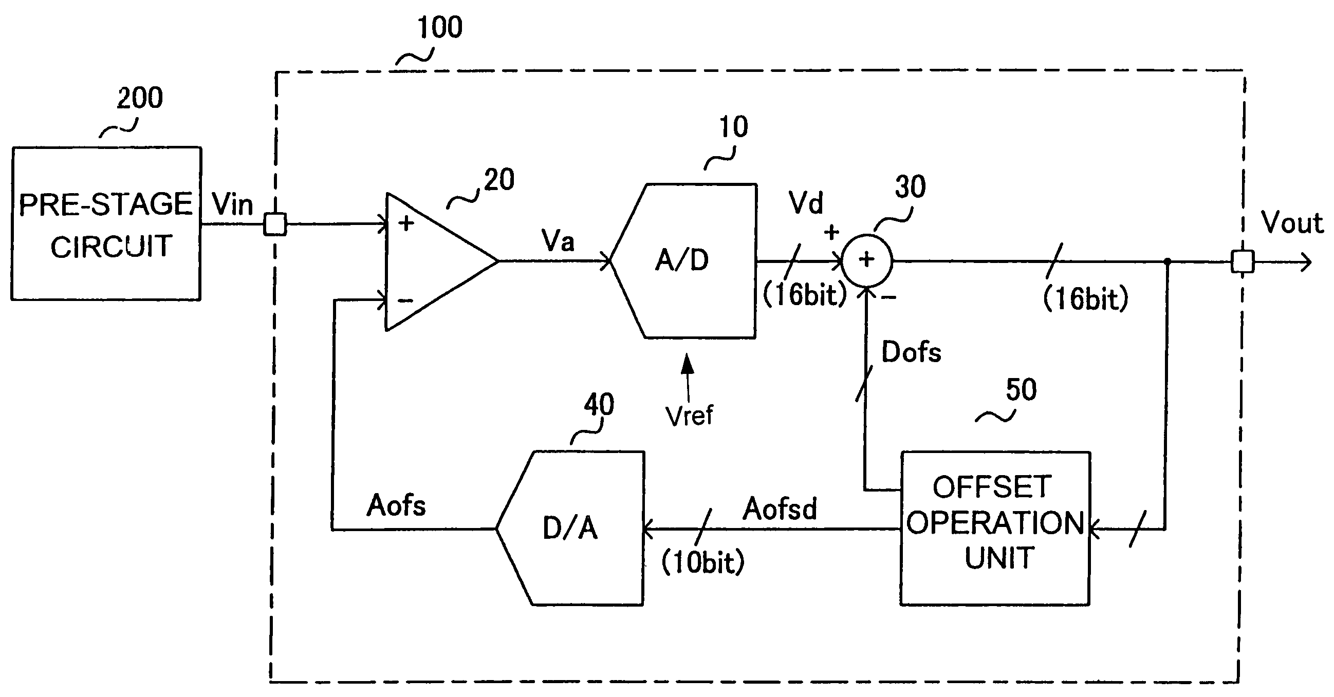
[0016]It is another object of the invention to provide an A / D conversion unit for converting an input voltage Vin, the A / D conversion unit having an offset canceling function adapted to cancel out the offset voltage contained in the central voltage Vctr of the input voltage Vin, the inventive A / D conversion unit thereby capable of correctly converting the input signal voltage Vsig contained in the input voltage into a digital signal if the central voltage is superimposed on the signal voltage Vsig.
[0041]Thus, the residual offset in the A / D conversion unit that cannot be removed by the analog offset canceller can be cancelled out or removed by the digital offset canceller, thereby allowing accurate A / D conversion.
[0042]Since the analog offset canceller is intended to eliminate a large portion of the offset voltage, including fluctuations of the input voltage which, presumably, has a predetermined level (i.e. central voltage), the analog offset canceller and the D / A converter can be of low accuracy, which allows reduction in size of the A / D conversion unit.
[0043]The number of data sampled for analog offset cancellation can be reduced by the invention, thereby reducing time for the offset cancellation.
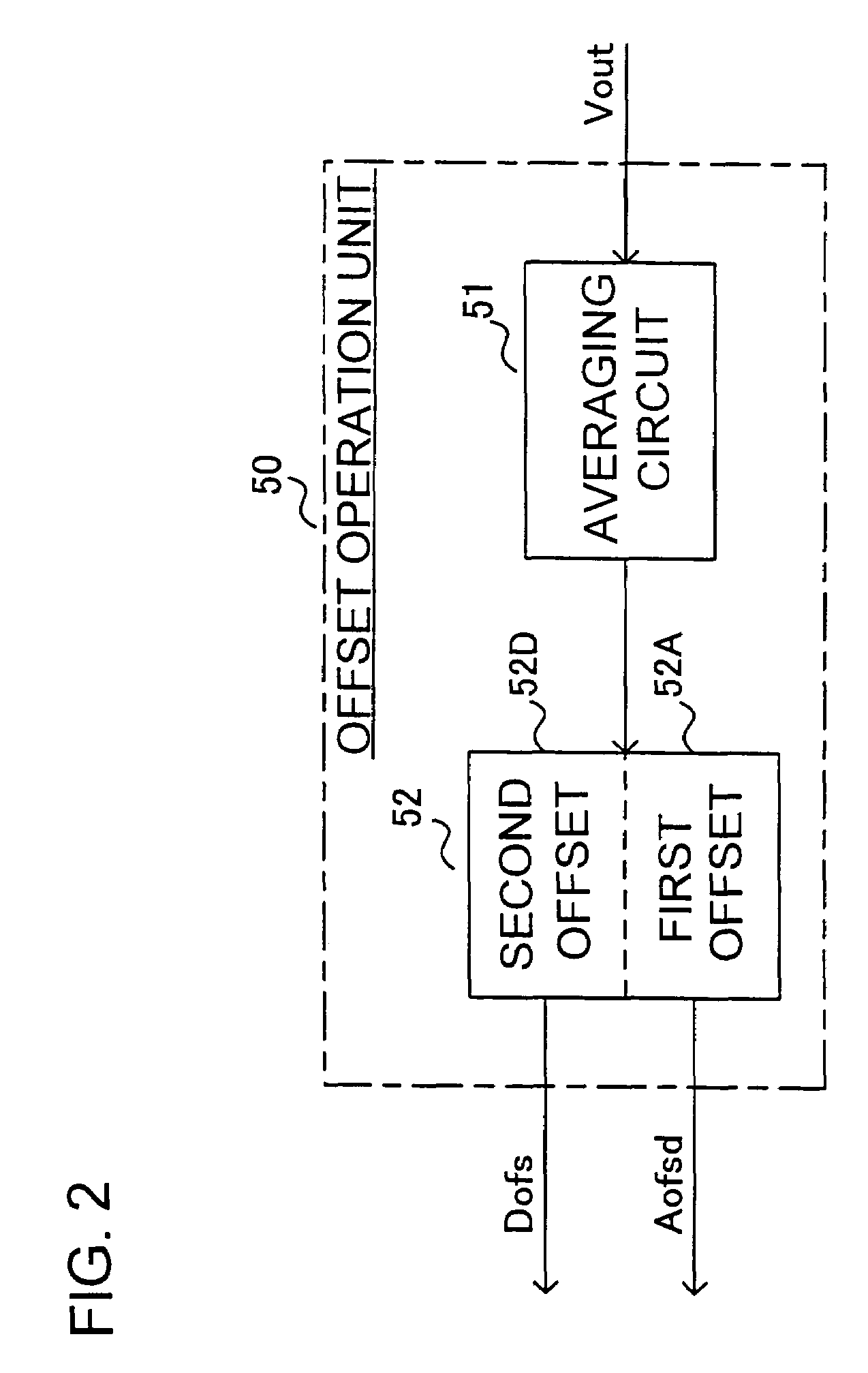
[0046]The use of a nonvolatile storage device as a memory 52 for storing the digitized analog offset canceling voltage Aofsd and digital offset canceling voltage Dofs enables readout of the stored offset canceling voltages Aofsd and Dofs from the nonvolatile storage device any time, once they are stored. Thus, the A / D conversion unit can provide accurate A / D conversion without repeating the procedure to obtain the voltages Aofsd and Dofs each time. Prior to shipping an inventive A / D conversion unit and / or communications apparatus to a user, the offset cancellation procedure can be performed to store the offset canceling voltages Aofsd and Dofs therefor in the nonvolatile storage device, thereby allowing the user to enjoy the use of a low-cost yet accurate A / D conversion unit and / or a communications apparatus equipped with an accurate A / D conversion unit.

Problems solved by technology

However, the A / D converter 60 of the A / D conversion unit disclosed in the cited patent application has a linearity error Vofs-ad.
Moreover, fluctuations Vofs-wn due to white noise also add to the errors.
Further reduction of the residual offset voltage can be anticipated by increasing the number of sampled data for offset cancellation, which, however, will require an adversely long time to obtain the offset canceling voltage.
Anyway, it is not possible with the prior art A / D conversion unit cited above to completely eliminate the offset voltage from the A / D conversion unit.
However, in obtaining the offset canceling voltage, the analog input voltage Vin is set to zero in the conventional A / D conversion unit, so that the offset voltage or the central voltage Vctr cannot be eliminated.
As a consequence, if the analog voltage Va saturates in the A / D conversion unit, the input voltage will be truncated (that is, its waveform will be clipped), thereby presenting an additional problem that the input signal voltage Vsig cannot be accurately converted into a correct digital signal.

Method used


Image

  • Analog to digital converter using both analog and digital offset voltages as feedback
  • Analog to digital converter using both analog and digital offset voltages as feedback
  • Analog to digital converter using both analog and digital offset voltages as feedback

Examples


Embodiment Construction

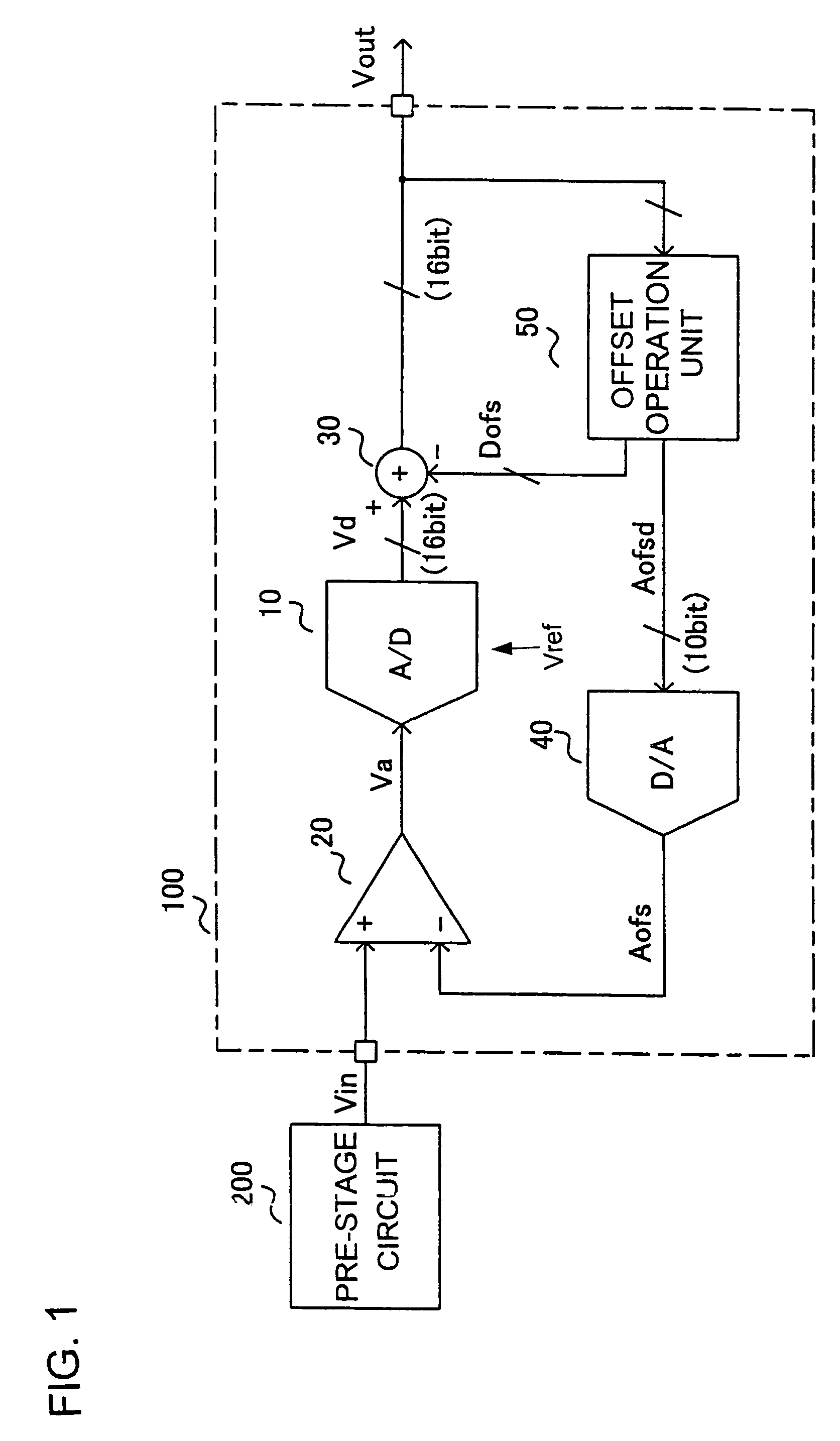
[0053]An A / D conversion unit having an offset canceling function according to one embodiment of the invention will now be described in detail, along with a communications apparatus utilizing such A / D conversion unit with reference to the accompanying drawings. As a communication apparatus, it would be best suited for applying to mobile apparatus, for example.

[0054]FIG. 1 shows an A / D conversion unit 100 and a pre-stage circuit 200 providing an analog input voltage Vin to the A / D conversion unit 100.

[0055]The pre-stage circuit 200 outputs for example an RF modulation signal, and, together with the A / D conversion unit 100, constitutes a communications apparatus. Under normal operating conditions, the pre-stage circuit 200 outputs an input signal voltage Vsig superimposed with a predetermined central voltage Vctr. To obtain an offset canceling voltage for the A / D conversion unit 100, only the central voltage Vctr is output from the pre-stage circuit 200.

[0056]An analog offset canceller...


PUM


Abstract

An A / D conversion unit includes an A / D converter, an analog offset canceller connected to the input end of the A / D converter, and a digital offset canceller connected to the output end of the A / D converter. The analog offset canceller performs a coarse adjustment of offset canceling voltage in the first stage of offset cancellation operation to largely cancel out the offset voltage involved in the A / D conversion unit by shifting the range of the input signal. Then the digital offset canceller performs a fine adjustment of offset canceling voltage in the second stage of offset cancellation operation to completely cancel out a residual offset voltage. Through the offset cancellation operation, the linearity error of the A / D converter, linearity error of the D / A converter, and matching error between the A / D and D / A converters are completely cancelled out.

Description

FIELD OF THE INVENTION[0001]This invention relates to an analog-to-digital (A / D) conversion unit having an offset canceling function, and to a communication unit, such as a mobile telephone, utilizing such A / D conversion unit.BACKGROUND OF THE INVENTION[0002]There have been known an A / D conversion unit having an offset canceling function for eliminating or canceling out the offset error involved in the A / D converter of the unit (see, for example, Japanese Patent Application Laid Open No. 2003-264462).[0003]FIG. 6 shows a circuit arrangement of an A / D conversion unit having a conventional offset canceling function as disclosed in FIG. 7 of the patent application cited above.[0004]As shown in FIG. 6, the A / D conversion unit has an A / D converter 60 for converting an analog input voltage Vin into a digital output voltage Vout, wherein, and hereinafter as well, digital voltage means voltage of a digitized signal.[0005]The A / D converter 60 has an offset error, which causes the A / D convert...

Claims


Application Information

Patent Timeline
Patent Type & Authority Patents(United States)
IPC IPC(8): H03M3/00
CPCH03M1/1019H03M1/10
Inventor SAWADA, AKINOBU
Owner ROHM CO LTD
Learn More