Method and system for ultrafast photoelectron microscope

a photoelectron microscope and ultra-fast technology, applied in the field of objects imaging, can solve the problems of not being able to obtain static images, giving us unparalleled insights into their static behavior, and unable to achieve static images currently available, and achieves the effect of low energy and easy implementation

Active Publication Date: 2006-12-26
CALIFORNIA INST OF TECH
View PDF3 Cites 47 Cited by
  • Summary
  • Abstract
  • Description
  • Claims
  • Application Information

AI Technical Summary

Problems solved by technology

The twentieth century has been witness to certain major advances in our ability to peer into the microscopic world of molecules, thereby giving us unparalleled insights into their static behavior.
Despite these advances in imaging, the dynamic aspects of structural evolution, insight into which is desirable in understanding function, cannot be obtained from currently available static images because of the lack of temporal resolution in conventional electron microscopy.
Unfortunately, limitations exist with conventional microscopic techniques.
As an example, conventional electron microscopes cannot generally produce images with spatial resolution on the biological length scale (ranging from nanometers to micrometers) with desirable temporal resolutions.

Method used


Image

  • Method and system for ultrafast photoelectron microscope
  • Method and system for ultrafast photoelectron microscope
  • Method and system for ultrafast photoelectron microscope

Examples


Embodiment Construction

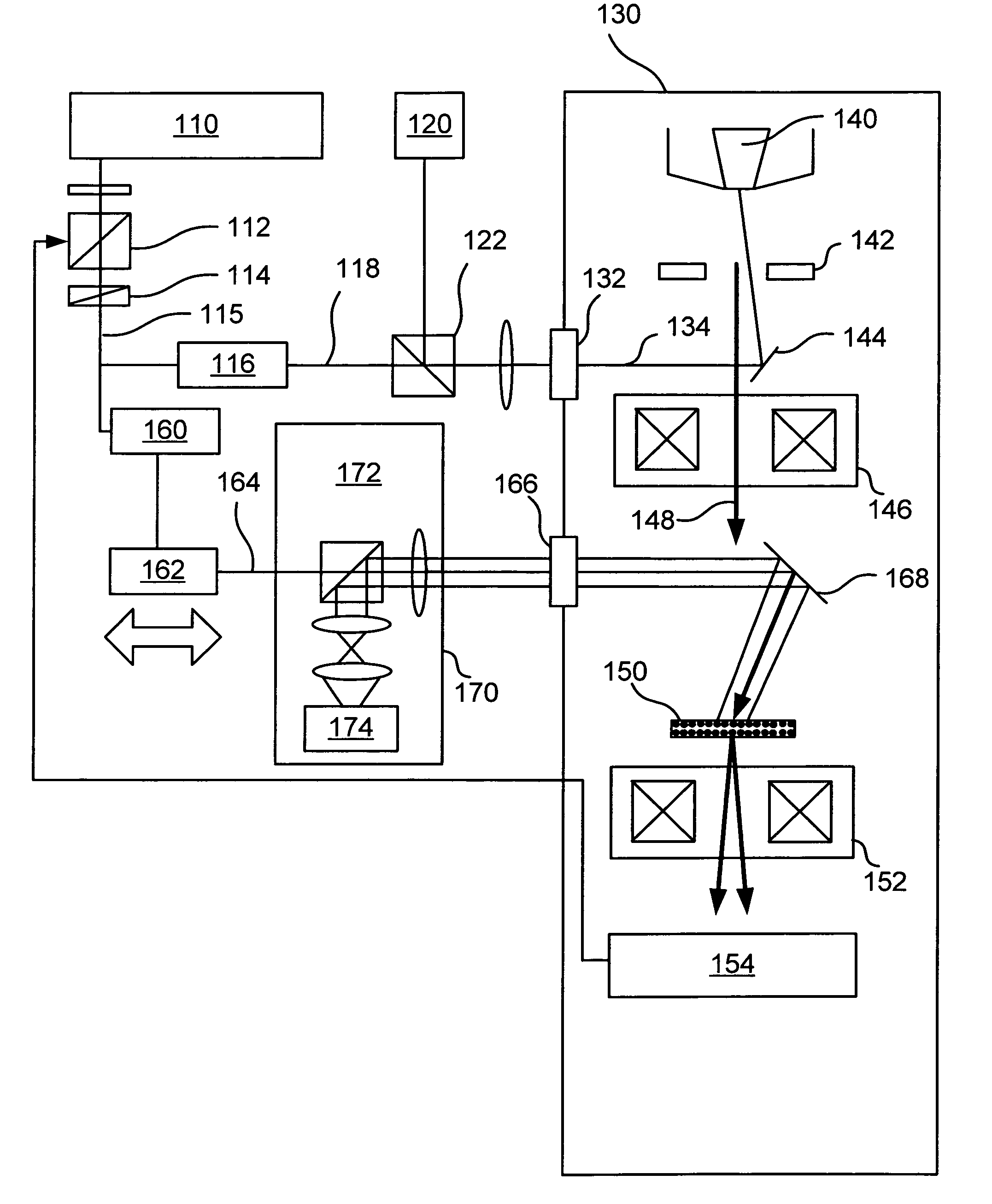
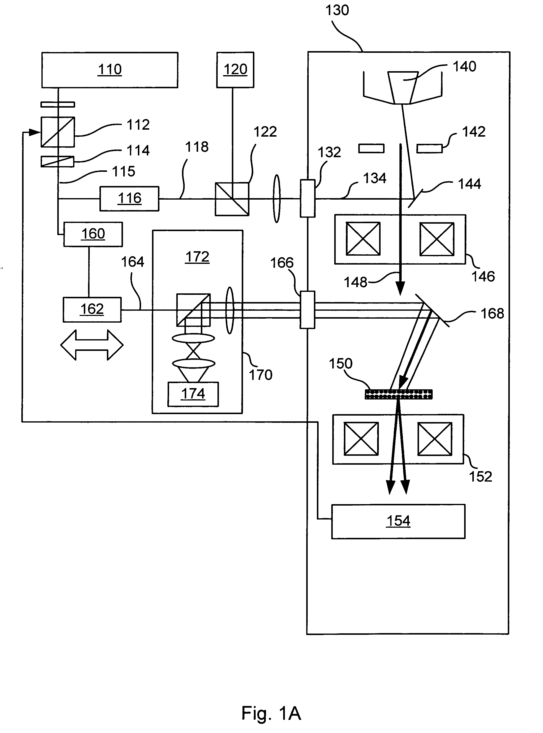
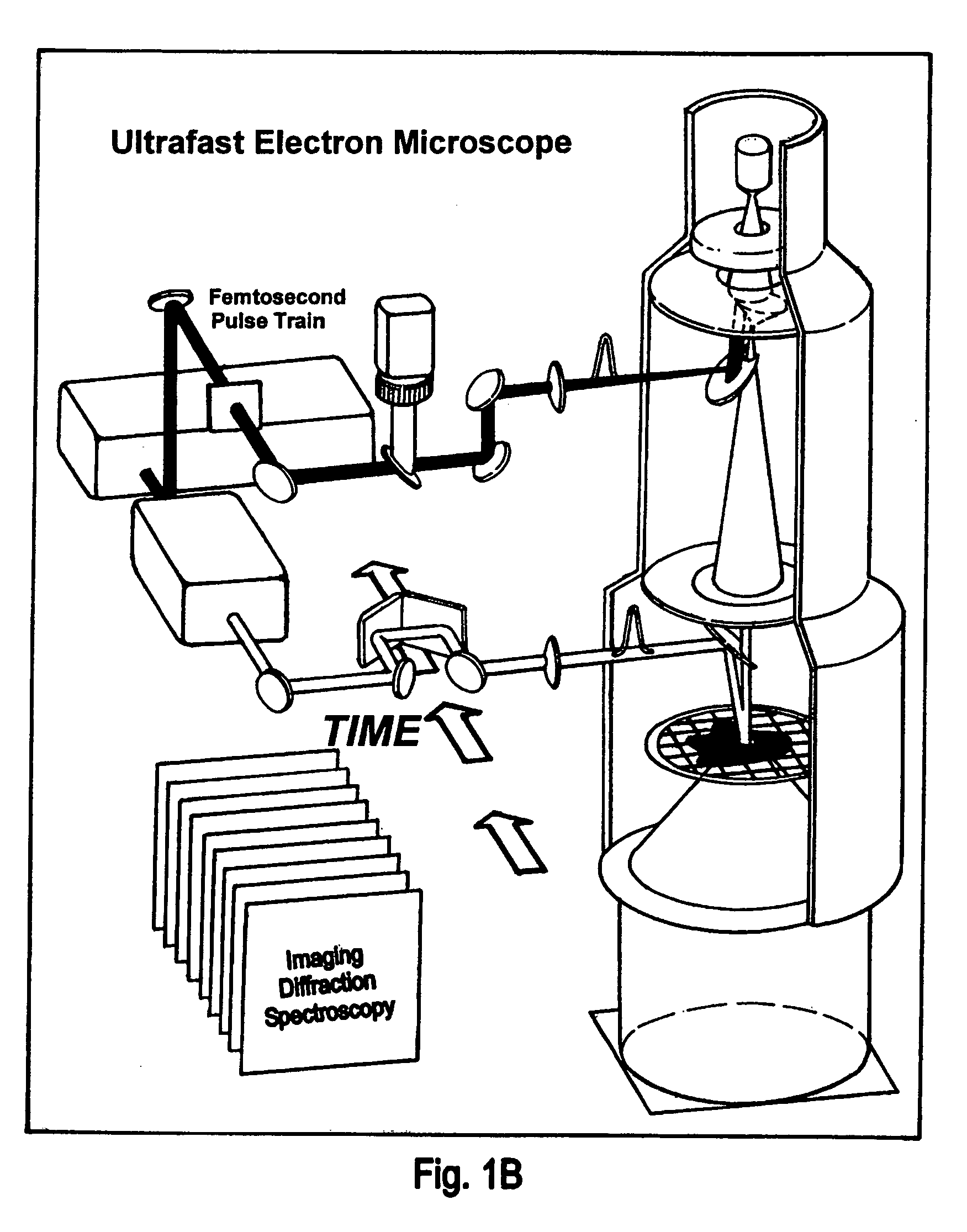
[0042]According to the present invention, techniques related to the imaging of objects are provided. In particular, the present invention provides methods and systems for imaging one or more objects using one or more pulses of particles containing from about one electron to about 10,000 electrons or more preferably about 10 electrons to about 100 electrons in a transmission electron microscope system. More particularly, the present invention provides methods and systems for identifying information about one or more temporal components associated with one or more spatial features of certain objects being imaged. Merely by way of example, the invention has been applied to imaging certain chemical, physical, and biological objects. The invention, however, can also be applied to other applications such as other areas of biology, chemistry (e.g., organic, physical, biochemistry), medicine (e.g., medical devices, diagnostics, analysis, treatments), physical sciences, electronics, semicond...


PUM

PropertyMeasurementUnit
temperatureaaaaaaaaaa
sizeaaaaaaaaaa
timeaaaaaaaaaa

Abstract

An ultrafast system (and methods) for characterizing one or more samples. The system includes a stage assembly, which has a sample to be characterized. The system has a laser source that is capable of emitting an optical pulse of less than 1 ps in duration. The system has a cathode coupled to the laser source. In a specific embodiment, the cathode is capable of emitting an electron pulse less than 1 ps in duration. The system has an electron lens assembly adapted to focus the electron pulse onto the sample disposed on the stage. The system has a detector adapted to capture one or more electrons passing through the sample. The one or more electrons passing through the sample is representative of the structure of the sample. The detector provides a signal (e.g., data signal) associated with the one or more electrons passing through the sample that represents the structure of the sample. The system has a processor coupled to the detector. The processor is adapted to process the data signal associated with the one or more electrons passing through the sample to output information associated with the structure of the sample. The system has an output device coupled to the processor. The output device is adapted to output the information associated with the structure of the sample.

Description

CROSS-REFERENCES TO RELATED APPLICATIONS[0001]This application claims the benefit of U.S. Provisional Application Ser. No. 60 / 559,234, filed Apr. 2, 2004, entitled “Ultrafast Photoelectron Microscope,” and U.S. Provisional Application Ser. Nos. 60 / 577,902, filed Jun. 7, 2004, entitled “Diffraction, Crystallography, and Microscopy beyond 3D—Structural Dynamics in Space and Time,” commonly assigned, and which are incorporated herein by reference.STATEMENT AS TO RIGHTS TO INVENTIONS MADE UNDER FEDERALLY SPONSORED RESEARCH OR DEVELOPMENT[0002]Work described herein has been supported, in part, by NSF grant CHE-0117850. The United States Government may therefore have certain rights in the invention.BACKGROUND OF THE INVENTION[0003]The present invention relates generally to imaging of objects. In particular, the present invention provides methods and systems for imaging one or more objects using one or more pulses of particles containing from about one electron to about 10,000 electrons or...

Claims


Application Information

Patent Timeline
Patent Type & Authority Patents(United States)
IPC IPC(8): H01J37/26G01N23/04H01J37/073
CPCH01J37/065H01J37/073H01J37/24H01J37/243H01J37/26H01J37/265H01J2237/0432H01J2237/06333H01J2237/06341H01J2237/206H01J2237/2065H01J2237/24585H01J2237/2482H01J2237/2803H01J2237/2809H01J2237/2813H01J2237/2855
Inventor ZEWAIL, AHMEDLOBASTOV, VLADIMIR
Owner CALIFORNIA INST OF TECH
Why Eureka
Try Eureka