
Card device, electronic apparatus, and wireless device

a card device and electronic equipment technology, applied in the direction of electronic wave modulation, printed circuit non-printed electric component association, modulation, etc., can solve the problems of difficult to mount two antennas in a separate fashion, problems similar to the foregoing, etc., to reduce the size of the card device, improve the convenience, and no additional load

Inactive Publication Date: 2006-10-17
PANASONIC CORP
View PDF30 Cites 11 Cited by
  • Summary
  • Abstract
  • Description
  • Claims
  • Application Information

AI Technical Summary

Benefits of technology

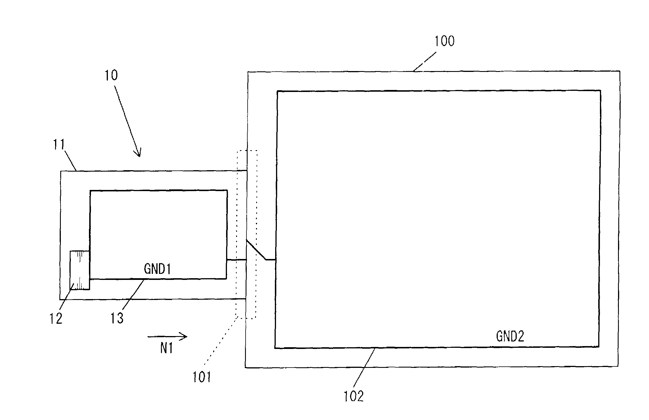
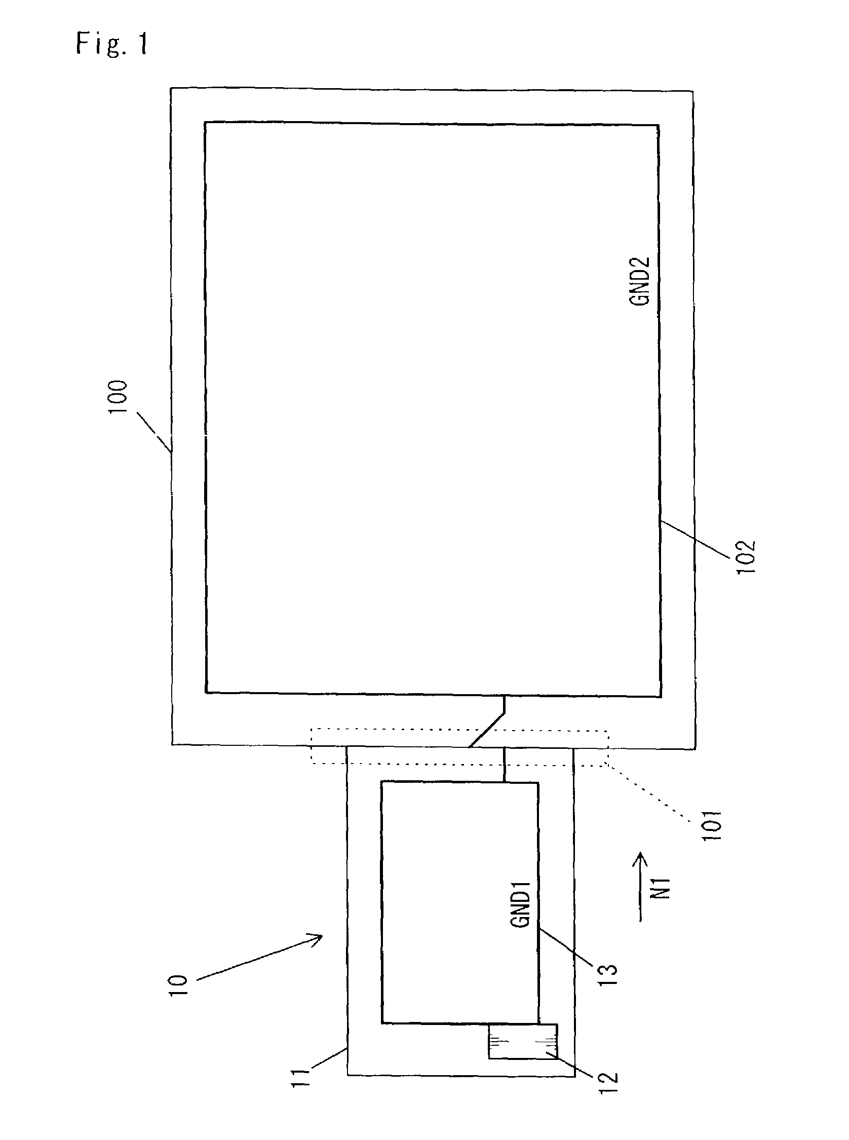
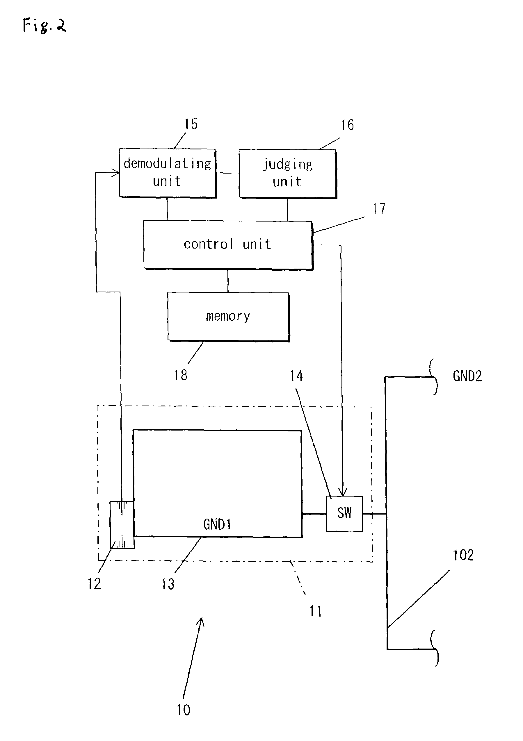
"The present invention provides a card device and a wireless device that can achieve the benefits of antenna diversity without using multiple antennas. The card device includes a carrier, a single antenna, a card ground, and a switch that can connect or disconnect the card ground to the electronic apparatus ground at a high frequency. The wireless device includes an antenna and a coupling element that can be adjusted to change the radiation characteristics of the antenna. The invention also includes a demodulating unit, a judging unit, and a control unit for controlling the switch. The invention further provides a construction that allows for the use of a small-sized antenna and the separation of the antenna and coupling element, reducing the size of the wireless device. The invention also includes a variable impedance device that can change the impedance between the coupling element and a ground point to achieve different radiation characteristics. The invention reduces the number of component types and costs associated with the construction of the wireless device."

Problems solved by technology

Satisfactory communications conditions are easily obtained when antenna diversity relieves harmful influences due to phasing.
However, if the device becomes smaller than this size, e.g., for reasons concerning space, it is difficult to mount two antennas in a separate fashion, and in most cases, only one antenna can be mounted.
In regard hereto, wireless devices having small-sized chips as antennas have been put into market circulation, however, even if such small-sized antennas are used, problems similar to the foregoing exist.

Method used


Image

  • Card device, electronic apparatus, and wireless device
  • Card device, electronic apparatus, and wireless device
  • Card device, electronic apparatus, and wireless device

Examples


example 1

[0069]FIG. 4 illustrates a mounting embodiment according to the second embodiment of the present invention. FIGS. 5(a) and 5(b) illustrate the radiation characteristics of antenna 20 resulting from the first mounting embodiment.

[0070]In this mounting embodiment, a laminated ceramic chip antenna 211, is used as the antenna 20. On one side of a printed circuit board 26, antenna 20 and laminated ceramic chip antenna 211 are arranged to be contiguous with each other so that laminated ceramic chip antenna 211 and antenna 20 are electrically coupled to each other.

[0071]The size of printed circuit board 26 is 50 mm long and 25 mm wide, and antenna 20 and laminated ceramic chip antenna 211, may be antenna model number YCE-5208 manufactured by YOKOWO, Co., Ltd. For variable impedance device 25, a switch model number UPG152TA manufactured by NEC Corporation may be used.

[0072]In addition, a measurement was carried out using a 2.44 GHz-frequency signal at a height of 2.5 meters from the floor s...

example 2

[0075]FIG. 6 illustrates another mounting embodiment for the second embodiment of the present invention. Unlike the previous mounting embodiment, for coupling element 21, a micro-strip line antenna formed by a circuit pattern of the printed circuit board 26 was used. Other aspects were identical to those of the first mounting embodiment. Also, the measurement example is illustrated in FIGS. 7(a) and 7(b).

[0076]As can be clearly understood in a comparison between FIG. 7(a) and FIG. 7(b), by turning the switch on or off, which corresponds to different impedances provided by variable impedance device 25, different radiation characteristics were obtained using a single antenna 20 (micro-strip line antenna 212 does not act as an antenna).

examples 3 and 4

[0077]In the first and second mounting embodiments, coupling element 21 specifications were known at the design phase and were used in the design of the device. However, as shown in FIG. 8 and FIG. 9, a coupling element 21 whose specifications are unknown at the design phase may also be used.

[0078]In the embodiment shown in FIG. 8, a connection point 213 having conductivity is provided on the side of the printed circuit board 26, and variable impedance device 25 is connected to connection point 213. Then, when this wireless device is attached to an electronic apparatus, such as a personal computer, variable impedance device 25 is connected to electronic apparatus ground 102 via connection point 213.

[0079]The above configuration results in a construction almost identical to the first embodiment, and by turning on or off variable impedance device 25, two types of radiation characteristics can be obtained using a single antenna 20.

[0080]Furthermore, as shown in FIG. 9(a), the present i...


PUM


Abstract

A card device to be inserted into a slot of an electronic apparatus having an electronic apparatus ground and electrically connected to this electronic apparatus, including a single antenna provided on a carrier, a card ground which is disposed on the carrier and electrically connected to the antenna, and a switch for carrying out, at a high frequency, a connection / disconnection of the card ground to / from the electronic apparatus ground in a condition where this card device is inserted in the slot.

Description

BACKGROUND OF THE INVENTION[0001]1. Field of the Invention[0002]The present invention relates to a small-sized card device to be detachably inserted into a slot of an electronic apparatus and, particularly, to a wireless device wherein effects of diversity can be obtained even with a small size.[0003]2. Description of the Related Art[0004]In recent years, wireless devices such as card devices which include antennas and provide electronic apparatuses with wireless communications functions have been widely used. Card devices of this type are typified by wireless LAN cards and card-type modems. In addition, card devices for the addition of wireless communications functions also provide additional system resources such as memories.[0005]In addition, wireless devices of this type include devices that have a plurality of antennas and in that antenna diversity has been realized. Satisfactory communications conditions are easily obtained when antenna diversity relieves harmful influences du...

Claims


Application Information

Patent Timeline
Patent Type & Authority Patents(United States)
IPC IPC(8): H04B1/38H04M1/00H01Q1/22H01Q1/38
CPCH01Q1/22H01Q1/38
Inventor KOGA, SHOUICHIKISHIMOTO, MICHINORIWAKISAKA, TOSHIYUKIWADA, MASAMI
Owner PANASONIC CORP
Learn More