
Selectively deferring instructions issued in program order utilizing a checkpoint and multiple deferral scheme

a technology of program order and deferral scheme, applied in the field of computer system performance improvement, can solve the problems of large fraction of waiting time of microprocessor systems, memory access speed of microprocessors, and large increase in clock speed of microprocessors, so as to facilitate extending out-of-order execution and simplify the rename unit. the effect of complexity

Active Publication Date: 2006-09-26
ORACLE INT CORP
View PDF6 Cites 23 Cited by
  • Summary
  • Abstract
  • Description
  • Claims
  • Application Information

AI Technical Summary

Benefits of technology

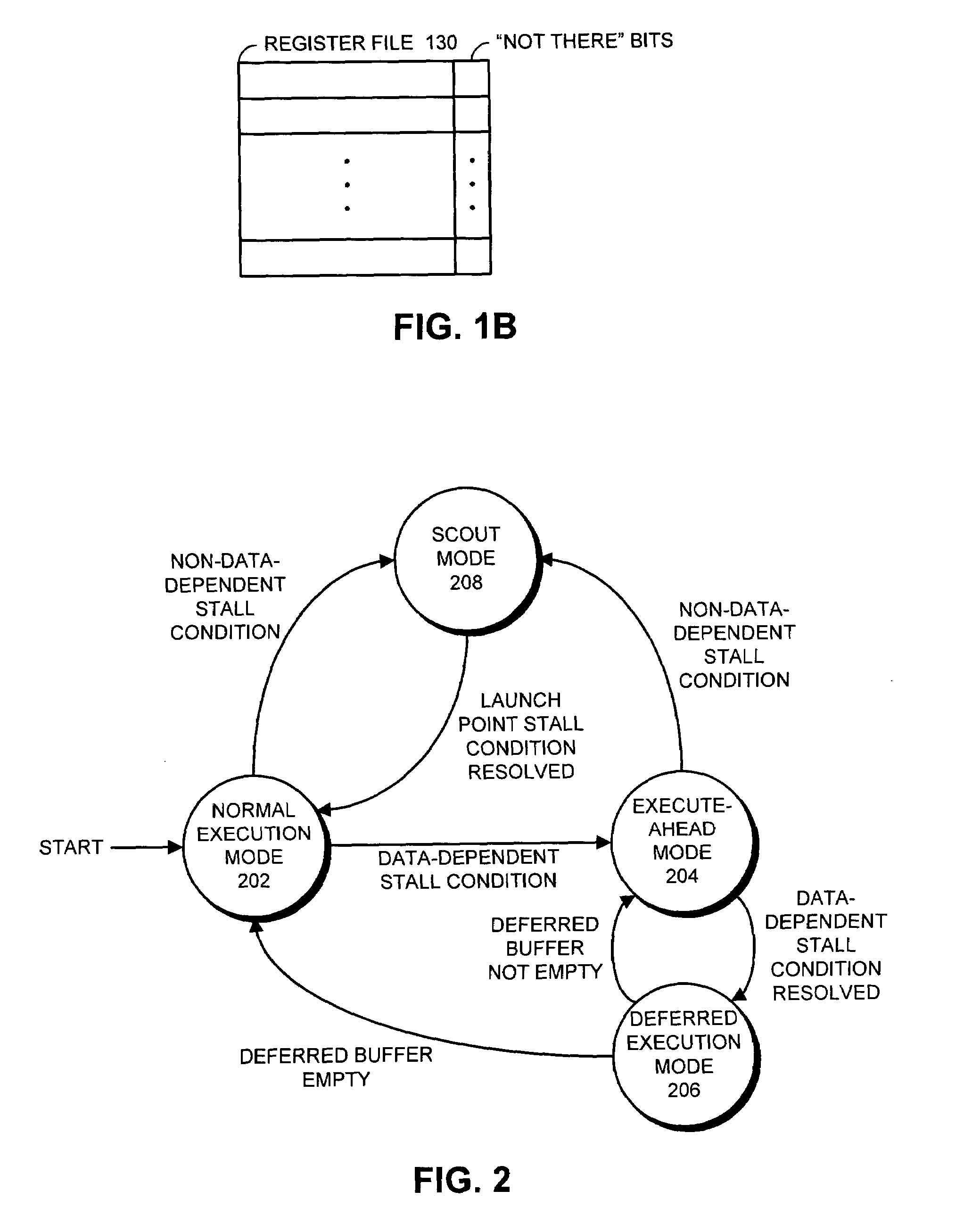
[0009]One embodiment of the present invention provides a system that facilitates deferring execution of instructions with unresolved data dependencies as they are issued for execution in program order. During a normal execution mode, the system issues instructions for execution in program order. Upon encountering an unresolved data dependency during execution of an instruction, the system generates a checkpoint that can subsequently be used to return execution of the program to the point of the instruction. Next, the system executes subsequent instructions in an execute-ahead mode, wherein instructions that cannot be executed because of an unresolved data dependency are deferred, and wherein other non-deferred instructions are executed in program order.
[0013]In a further variation, generating the checkpoint involves saving the precise architectural state of the processor to facilitate subsequent recovery from exceptions that arise during execute-ahead mode or deferred mode.
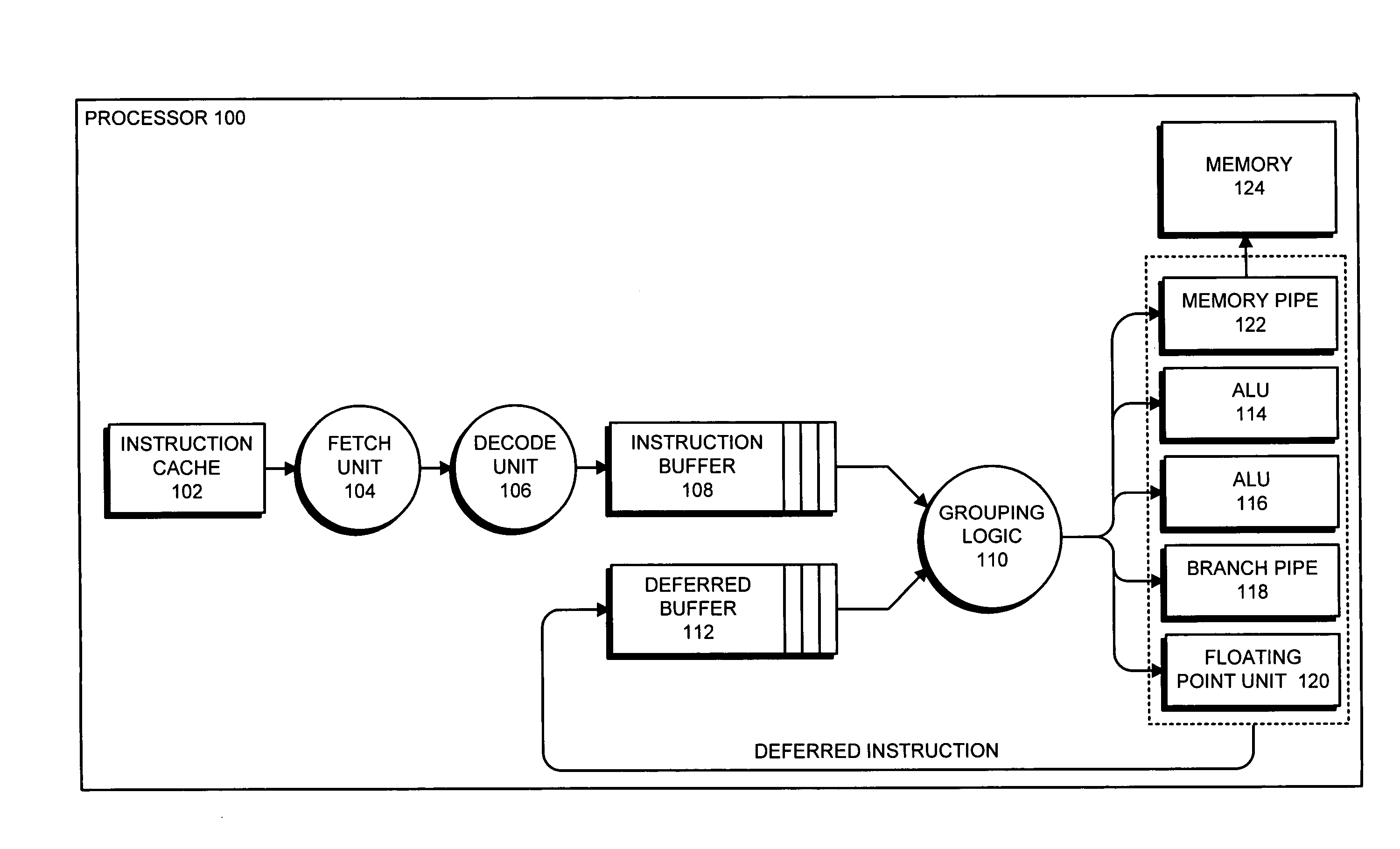
[0020]Note that the present invention has a number of advantages over traditional out-of-order designs. First, the instruction buffers are simple first-in-first-out (FIFO) buffers, which unlike conventional out-of-order execution windows, do not require complex circuitry for content-addressable-memory (CAM) operations. Moreover, the FIFO buffers are common SRAM cells with a single read port and a single write port. Thus, their area grows linearly with their size, and hence permits storage of thousands of deferred instructions. In fact, given the density advantages of SRAM, these thousands of instructions can be stored in the same area as is used by a traditional out-of-order issue queue, which may only store only 128 instruction. (Note that although the above-described embodiment of the present invention uses FIFO buffers to implement both instruction buffer 108 and deferred buffer 112, other non-FIFO structures, such as SRAM, can be used to implement instruction buffer 108 and deferred buffer 112.)
[0021]Second, only dependent instructions are retained in the deferred buffer, because independent data-ready instructions are executed at once. This saves chip resources. Note that in traditional out-of-order designs, data-ready instructions that have issued continue to consume space in the issue queue (or equivalent structure) until they are retired.
[0022]Moreover, renaming of architectural registers to physical registers is not necessary, and so the complexity of the rename unit can be dispensed with. This means that the size of the out-of-order window is not limited by the register file size. Hence, the present invention facilitates extending out-of-order execution to a potentially unlimited number of instructions.

Problems solved by technology

Hence, the disparity between microprocessor clock speeds and memory access speeds continues to grow, and is beginning to create significant performance problems.
This means that the microprocessor systems spend a large fraction of time waiting for memory references to complete instead of performing computational operations.
However, when a memory reference, such as a load operation generates a cache miss, the subsequent access to level-two (L2) cache or memory can require dozens or hundreds of clock cycles to complete, during which time the processor is typically idle, performing no useful work.
Unfortunately, existing out-of-order designs have a hardware complexity that grows quadratically with the size of the issue queue.
Practically speaking, this constraint limits the number of entries in the issue queue to one or two hundred, which is not sufficient to hide memory latencies as processors continue to get faster.
Moreover, constraints on the number of physical registers that are available for register renaming purposes during out-of-order execution also limits the effective size of the issue queue.
However, it suffers from the disadvantage of having to re-compute any computational operations that are performed while in scout-ahead mode.

Method used


Image

  • Selectively deferring instructions issued in program order utilizing a checkpoint and multiple deferral scheme
  • Selectively deferring instructions issued in program order utilizing a checkpoint and multiple deferral scheme
  • Selectively deferring instructions issued in program order utilizing a checkpoint and multiple deferral scheme

Examples


Embodiment Construction

[0026]The following description is presented to enable any person skilled in the art to make and use the invention, and is provided in the context of a particular application and its requirements. Various modifications to the disclosed embodiments will be readily apparent to those skilled in the art, and the general principles defined herein may be applied to other embodiments and applications without departing from the spirit and scope of the present invention. Thus, the present invention is not intended to be limited to the embodiments shown, but is to be accorded the widest scope consistent with the principles and features disclosed herein.

Processor

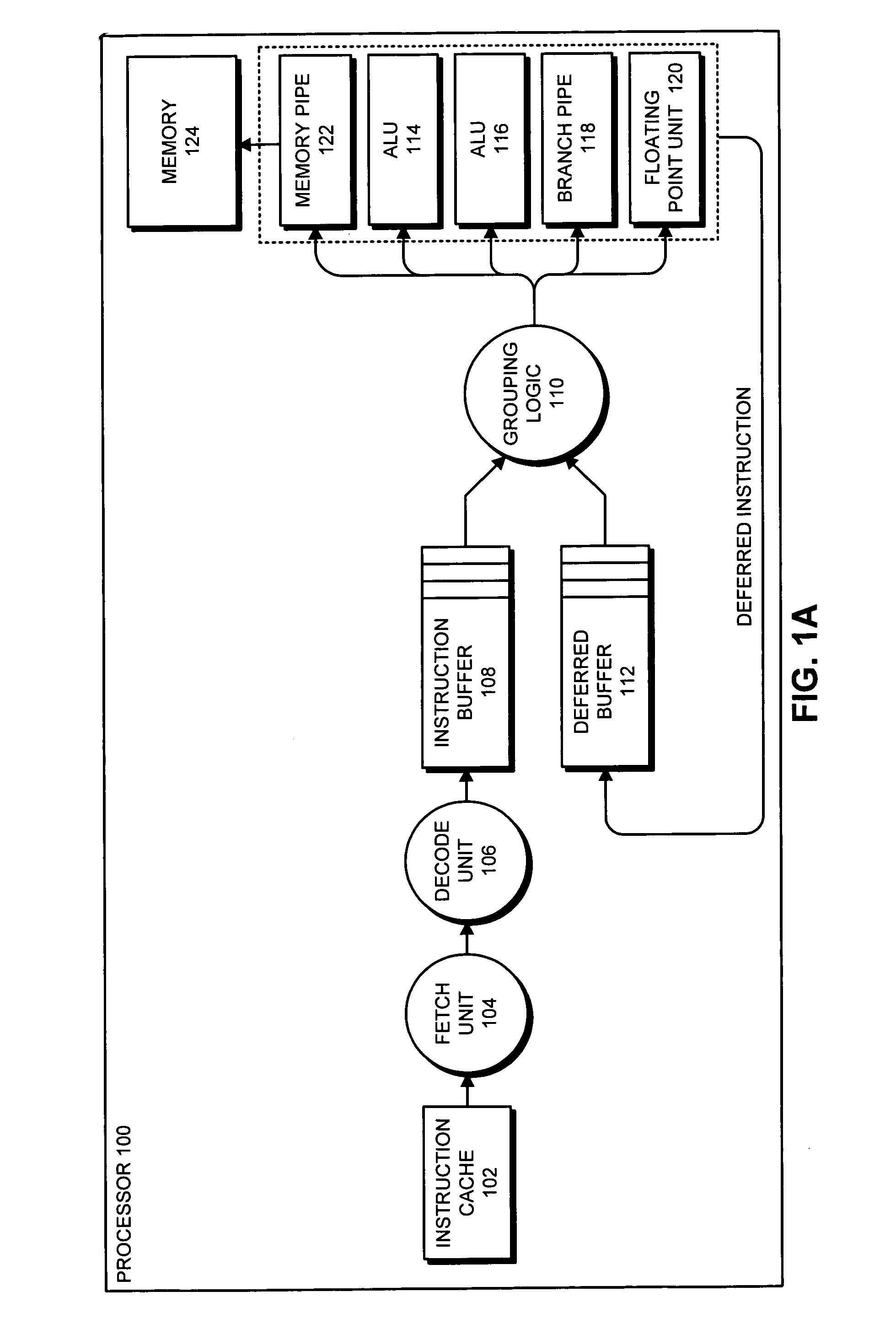
[0027]FIG. 1A illustrates the design of a processor 100 in accordance with an embodiment of the present invention. Processor 100 can generally include any type of processor, including, but not limited to, a microprocessor, a mainframe computer, a digital signal processor, a personal organizer, a device controller and a computational en...


PUM


Abstract

One embodiment of the present invention provides a system that facilitates deferring execution of instructions with unresolved data dependencies as they are issued for execution in program order. During a normal execution mode, the system issues instructions for execution in program order. Upon encountering an unresolved data dependency during execution of an instruction, the system generates a checkpoint that can subsequently be used to return execution of the program to the point of the instruction. Next, the system executes subsequent instructions in an execute-ahead mode, wherein instructions that cannot be executed because of an unresolved data dependency are deferred, and wherein other non-deferred instructions are executed in program order.

Description

BACKGROUND[0001]1. Field of the Invention[0002]The present invention relates to techniques for improving the performance of computer systems. More specifically, the present invention relates to a method and an apparatus for speeding up program execution by selectively deferring execution of instructions with unresolved data-dependencies as they are issued for execution in program order.[0003]2. Related Art[0004]Advances in semiconductor fabrication technology have given rise to dramatic increases in microprocessor clock speeds. This increase in microprocessor clock speeds has not been matched by a corresponding increase in memory access speeds. Hence, the disparity between microprocessor clock speeds and memory access speeds continues to grow, and is beginning to create significant performance problems. Execution profiles for fast microprocessor systems show that a large fraction of execution time is spent not within the microprocessor core, but within memory structures outside of t...

Claims


Application Information

Patent Timeline
Patent Type & Authority Patents(United States)
IPC IPC(8): G06F9/38G06F9/00G06F9/45
CPCG06F9/3836G06F9/3838G06F9/3842G06F9/384G06F9/3865G06F9/3855G06F9/3857G06F9/3863G06F9/3856G06F9/3858
Inventor CHAUDHRY, SHAILENDERTREMBLAY, MARC
Owner ORACLE INT CORP
Learn More