Magnetic nonvolatile memory cell and magnetic random access memory using the same
a non-volatile memory and magnetic random access technology, applied in the direction of digital storage, instruments, semiconductor devices, etc., can solve the problem of not being able to reduce the power needed
- Summary
- Abstract
- Description
- Claims
- Application Information
AI Technical Summary
Benefits of technology
Problems solved by technology
Method used
Image
Examples
first embodiment
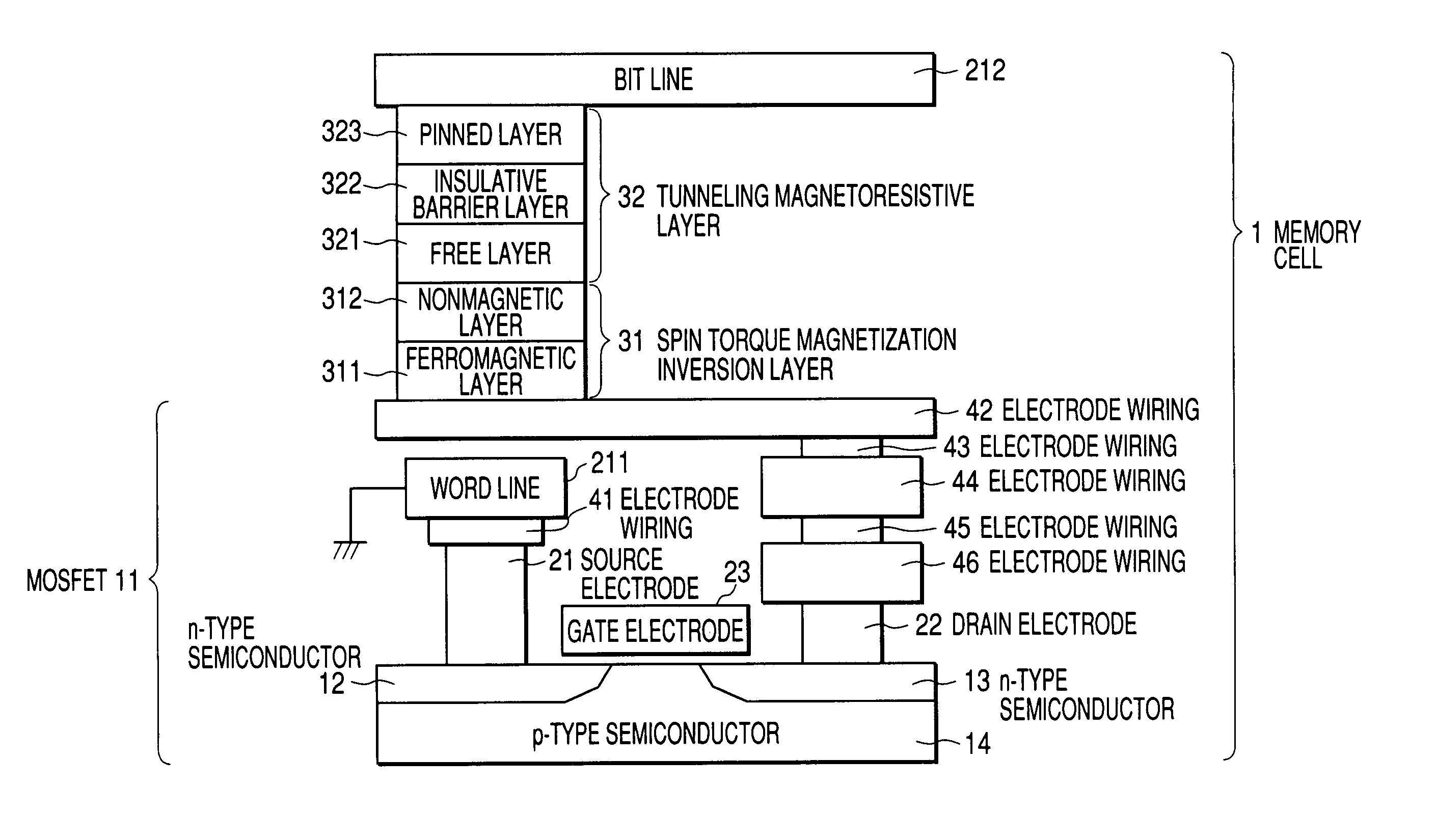
[0019]FIG. 1 is a schematic sectional view of an embodiment of the magnetic nonvolatile memory cell (hereinafter briefly referred to as “memory cell”) of the present invention. A C-MOSFET 11 comprises two n-type semiconductors 12 and 13, and one p-type semiconductor 14. A source electrode 21 is electrically connected to the n-type semiconductor 12 and to a word line constituting the magnetic memory. A drain electrode 22 is electrically connected to the n-type semiconductor 13. The electric current passing between the source electrode 21 and the drain electrode 22 is switched on and off by switching on and off of a gate electrode 23. The n-type semiconductors and p-type semiconductor used herein are semiconductors containing Si.
[0020]A spin torque magnetization inversion layer 31 is arranged above the C-MOSFET 11 and is electrically connected to an electrode wiring 42. The spin torque magnetization inversion layer 31 includes a ferromagnetic layer (first ferromagnetic layer) 311 and ...
second embodiment
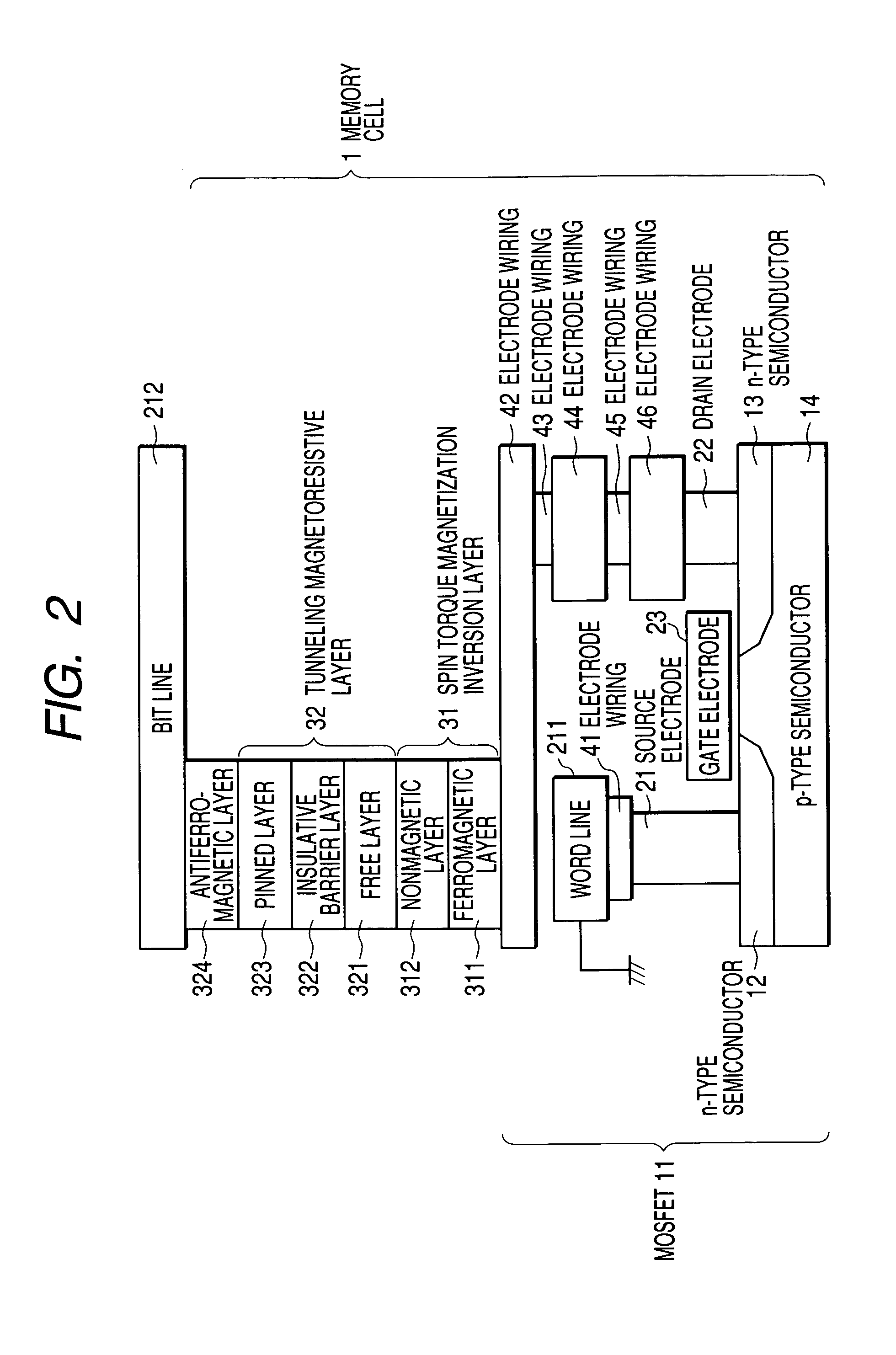
[0025]FIG. 2 is a schematic sectional view of a memory cell 1 having the configuration of FIG. 1, except for further comprising an antiferromagnetic layer 324 for fixing the magnetization direction of the pinned layer 323 in one direction. The antiferromagnetic layer 324 herein comprises a PtMn film 12 nm thick. Alternatively, an IrMn or FeMn film can be used for the antiferromagnetic layer 324. The antiferromagnetic layer 324 contributes to stabilize the antiparallel and parallel arrangement of the magnetization directions of the pinned layer 323 and the free layer 321 to thereby increase the output of the tunneling magnetoresistive layer 32. The memory cell according to Second Embodiment shows resistance-electric current properties with hysteresis as shown in FIG. 5. The tunneling magnetoresistive layer 32 in this embodiment has an output of 50%, higher than the memory cell of First Embodiment.
[0026]A magnetic random access memory comprising a plurality of the magnetic nonvolatile...
third embodiment
[0027]FIG. 3 is a schematic sectional view of another embodiment of a memory cell 1 according to the present invention. In this embodiment, the C-MOSFET 11 comprises a substrate, and an n-type semiconductor 131 serving as a source electrode, a p-type semiconductor 141, and an n-type semiconductor 121 serving as a drain electrode arranged in this order in a perpendicular direction to the substrate plane. The gate electrode 23 is arranged around but not in direct contact with the p-type semiconductor 141. The spin torque magnetization inversion layer 31 and the tunneling magnetoresistive layer 32 are arranged on or above the n-type semiconductor 121. Their materials, thickness and lamination order are the same as First Embodiment.
[0028]According to Third Embodiment, by perpendicularly arranging the n-type semiconductor 121 serving as the drain electrode and n-type semiconductor 131 serving as the source electrode, and arranging the gate electrode 23 on the side wall of the cell, the r...
PUM
 Abstract
Description
Claims
Application Information
 - Generate Ideas
- Intellectual Property
- Life Sciences
- Materials
- Tech Scout
- Unparalleled Data Quality
- Higher Quality Content
- 60% Fewer Hallucinations
Browse by: Latest US Patents, China's latest patents, Technical Efficacy Thesaurus, Application Domain, Technology Topic, Popular Technical Reports.
© 2025 PatSnap. All rights reserved.Legal|Privacy policy|Modern Slavery Act Transparency Statement|Sitemap|About US| Contact US: help@patsnap.com


