
Solving constraint satisfiability problem for circuit designs

a constraint and constraint satisfiability technology, applied in the field of functional verification of circuit designs, can solve the problems of expensive re-spin of the design process, manual generation of verification vectors by designers, and the most time-consuming component of verification

Inactive Publication Date: 2006-07-04
CADENCE DESIGN SYST INC
View PDF9 Cites 22 Cited by
  • Summary
  • Abstract
  • Description
  • Claims
  • Application Information

AI Technical Summary

Benefits of technology

[0014]For purposes of summarizing the invention, certain aspects, advantages, and novel features of the invention have been described herein. It is to be understood that not necessarily all such advantages may be achieved in accordance with any one particula

Problems solved by technology

Verification is typically the most time-consuming component in a circuit design process.
Failing to detect functional design errors early in the design stage usually leads to the expensive re-spin of the design process.
A drawback is that the verification vectors are either manually derived by designers or randomly generated from the high-level description of the design and its environment.
As a result, verification vectors, for example, for some corner-case bugs, are not easily derived and high coverage is generally hard to achieve.
However, due to the increasing complexity of modem circuit designs, current constraint satisfiability techniques still suffer from unacceptable capacity and performance problems.
However, because the computational complexity of these techniques grows exponentially as the sequentiality of the property increases, these techniques can only handle property checking with limited sequential depth.
However, since the signal values of the circuit actually operate in the modular number system, solving circuit constraints in the integral or floating point number system may add unnecessary complexity and even lead to invalid solutions.
Since the number of states grows exponentially as the number of registers increases, the explicit state enumeration technique has the state explosion problem for larger designs.
However, symbolic state traversal approach still suffers from the state explosion problem for designs with more than approximately one hundred registers.
As a result, full chip (whole circuit) functional verification is unattainable using FSM state traversal techniques.

Method used


Image

  • Solving constraint satisfiability problem for circuit designs
  • Solving constraint satisfiability problem for circuit designs
  • Solving constraint satisfiability problem for circuit designs

Examples


example

[0123]The detailed procedure of the linear constraint-solving algorithm is illustrated using the following linear circuit example:

[0124]

[0125]Assume all the signal buses of the above linear circuit example are 4-bits wide and the initial assignments for output x=2 and y=10 are given. The linear constraints can be expressed as an integer matrix equation:

[0126][3-10-212-20]·[abcd]=[210]

Modulating the coefficients by 16(24) produces:

[0127][31501412140]·[abcd]=[210]

[0128]First, a (series of) row operation(s) is performed to upper-trianglize the matrix; that is, make its lower-left element(s) 0. Here, the first row of the above example is multiplied by the multiplicative inverse of its first element (i.e., multiplicative_inverse(3) 11) and subtracted from the second row. The equation then becomes:

[0129][315014013146]·[abcd]=[24]

[0130]The partial solution for the last nonzero row is then solved. To obtain a particular solution for a single-row equation, a check to determine if the greates...


PUM


Abstract

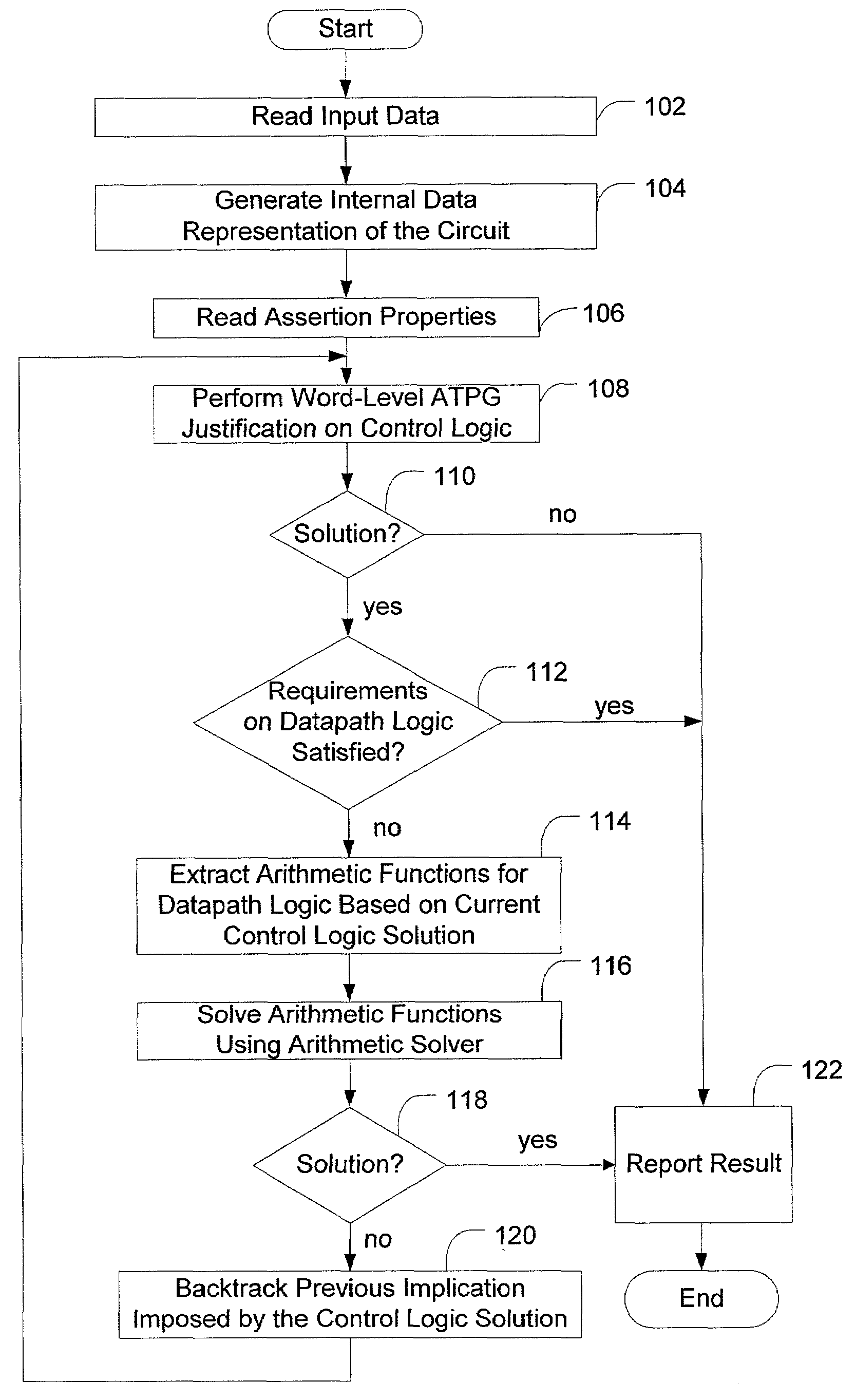
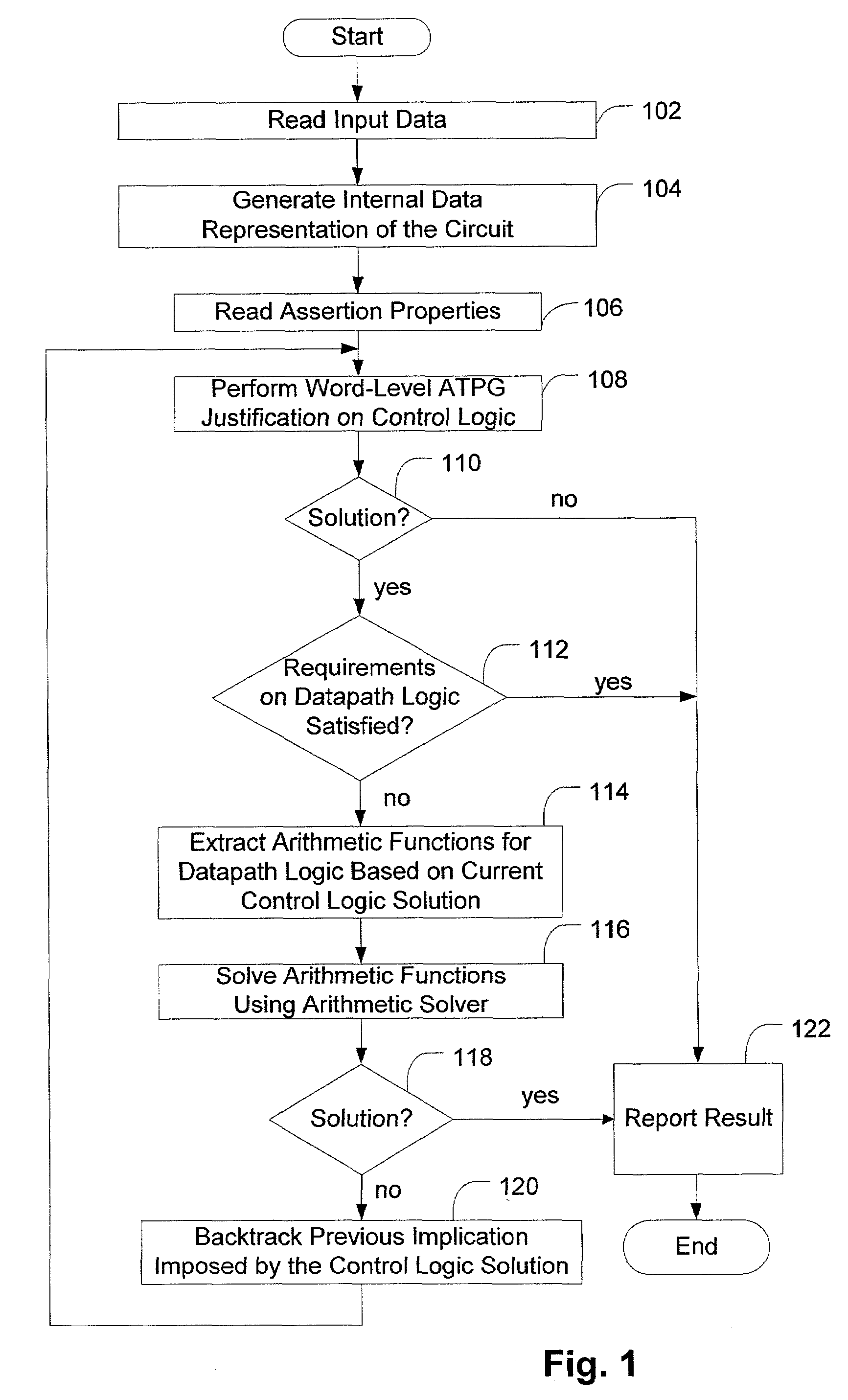
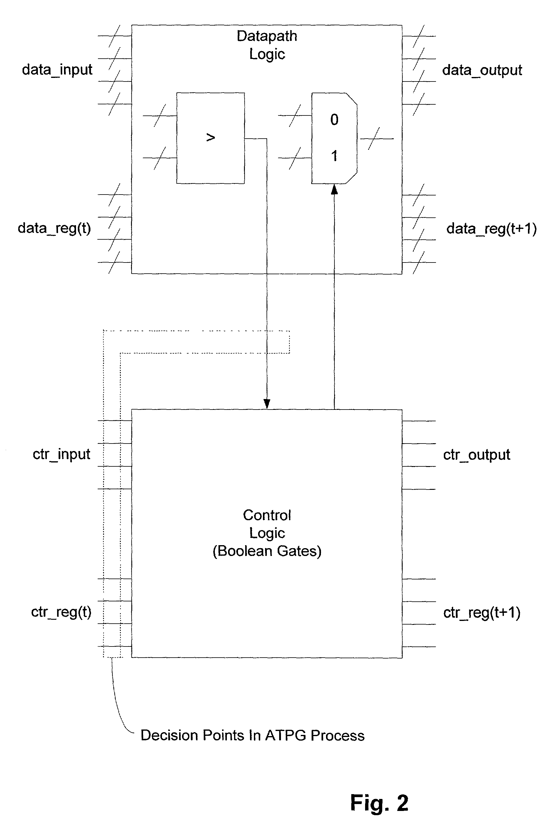
A method for generating a test vector for functional verification of circuits includes providing a representation of a circuit, where the representation includes a control logic component and a datapath logic component. The method also includes reading one or more vector generation targets, and performing word-level ATPG justification on the control logic component to obtain a control logic solution. The method further includes extracting one or more arithmetic functions for the datapath logic component based on the control logic solution, and solving the one or more arithmetic functions using a modular constraint solver. The modular constraint solver is based on a modular number system.

Description

CLAIM FOR PRIORITY[0001]This application claims the benefit of priority under 35 U.S.C. § 119(e) of U.S. Provisional Application No. 60 / 246,422 filed on Nov. 6, 2000, the entirety of which is incorporated herein by reference.APPENDICES[0002]Appendix A, which forms a part of this disclosure, provides theoretic details of the modular constraint solver as disclosed herein.[0003]Appendix B, which forms a part of this disclosure, provides an exemplary procedure for solving linear equations that have bit slicing and concatenation operations.BACKGROUND[0004]1. Field[0005]The present invention relates generally to functional verification of circuit designs and, more particularly, to the generation of verification vectors for use in debugging circuit designs.[0006]2. Description of the Related Art[0007]Verification is typically the most time-consuming component in a circuit design process. Failing to detect functional design errors early in the design stage usually leads to the expensive re-...

Claims


Application Information

Patent Timeline
IPC IPC(8): G06F17/50
CPCG06F17/504G06F30/3323
Inventor HUANG, CHUNG-YANG
Owner CADENCE DESIGN SYST INC
Learn More