
Flash ADC with variable LSB

a technology of flash converter and variable, applied in the field of data converter, can solve the problems of limiting flash converters to high frequency applications that typically cannot be addressed in any other way, consuming a lot of power, and relatively low resolution

Inactive Publication Date: 2006-06-13
SILICON LAB INC
View PDF13 Cites 29 Cited by
  • Summary
  • Abstract
  • Description
  • Claims
  • Application Information

AI Technical Summary

Problems solved by technology

However, Flash converters consume a lot of power, have relatively low resolution, and can be quite expensive.
This limits them to high frequency applications that typically cannot be addressed any other way.
It is difficult to obtain both wide bandwidth and high gain.
Otherwise, the offset of the comparator could falsely trip the comparator, resulting in a digital output code not representative of a thermometer code.
An increase in die size increases cost.
As compared to a SAR ADC, the Flash ADC is more expensive.
However, each pipelined stage is much slower than a Flash section.
However, some Flash converters require a pre-amplifier to drive the comparators.

Method used


Image

  • Flash ADC with variable LSB
  • Flash ADC with variable LSB
  • Flash ADC with variable LSB

Examples


Embodiment Construction

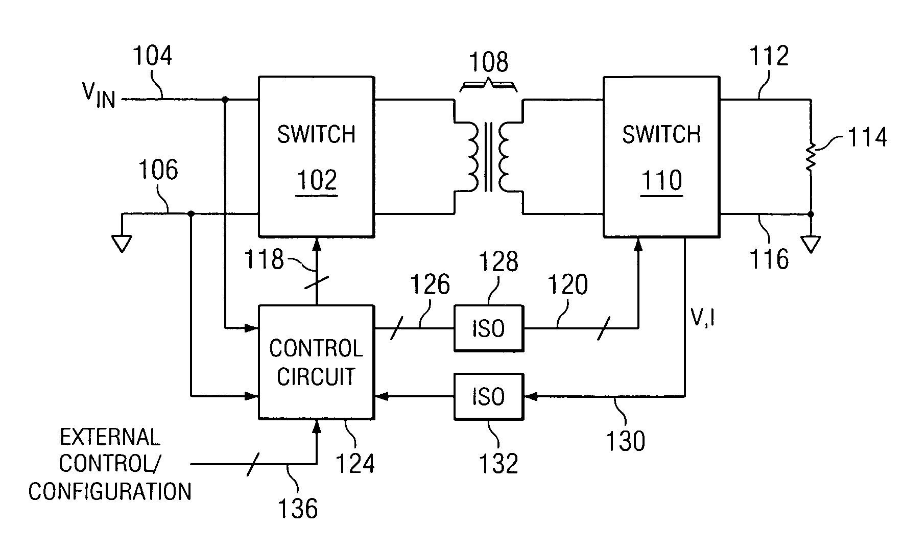
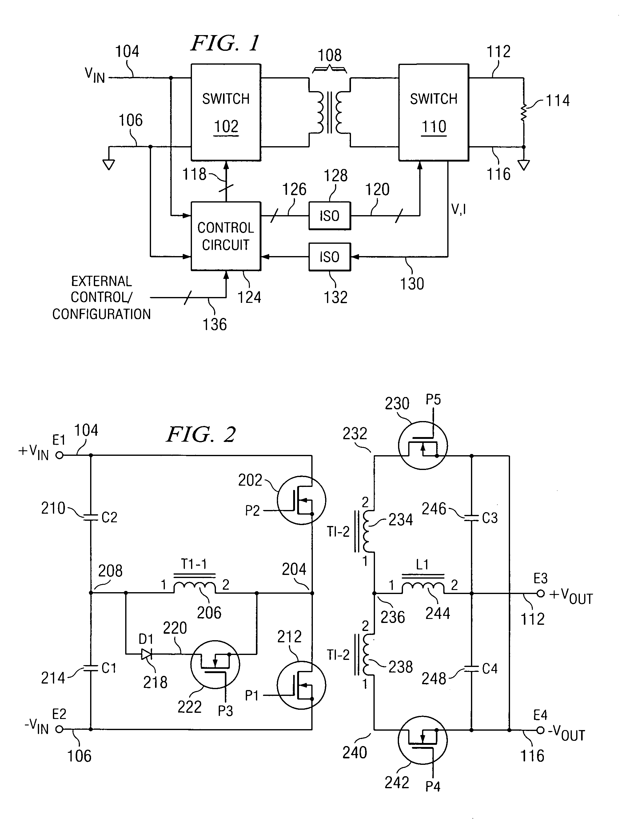
[0026]Referring now to FIG. 1, there is illustrated a top level schematic diagram for the switching power supply of the present embodiment. The main portion of the power supply comprises a primary switch group 102 that is operable to receive an input voltage on a node 104, this being a DC voltage, and ground on a node 106. The primary switch group 102 is coupled through an isolation transformer 108 to a secondary switch group 110. The secondary switch group 110 is operable to drive an output voltage node 112 that is connected to one terminal of a load 114, the secondary switch group 110 also having a ground connection on a node 116, the load 114 disposed between the node 112 and the node 116. The two switch groups 102 and 110 are operable to operate in conjunction with various pulse inputs on a control bus 118 associated with the primary switch group 102 and with various pulse inputs on a control bus 126 associated with the secondary switch group 110.

[0027]A digital control circuit ...


PUM


Abstract

A differential analog-to-digital data converter (ADC) is disclosed for receiving a positive input signal and a negative input signal. A distributed resistive device is provided having taps associated therewith. A plurality of comparators each having a signal input and a reference input are provided, the signal input connected to one of the positive and negative input signals and the reference input connected to a tap on said distributed resistive device. A driver drives current through the distributed resistive device with one of the taps of the distributed resistive device disposed at substantially the other of the positive and negative input signals. A current varying device varys the current through the distributed resistive device to vary the voltage between taps.

Description

[0001]This application is related to U.S. patent application Ser. No. 11 / 095,844, filed date herewith, and entitled “DIGITAL PULSE WIDTH MODULATED POWER SUPPLY VARIABLE LSB” and U.S. patent application Ser. No. 11 / 096,597, filed of even date herewith, and entitled “DIGITAL PWM CONTROLLER”, both of which are incorporated herein by reference in their entirety.TECHNICAL FIELD OF THE INVENTION[0002]The present invention pertains in general to data converters and, more particularly, to analog-to-digital converters (ADCs) of the Flash type.BACKGROUND OF THE INVENTION[0003]There are various types of ADC architectures, one of which is the Flash ADC. These are sometimes known as parallel ADCs. They are considered the fastest way to convert an analog signal to a digital signal. They are suitable for applications requiring very large bandwidths. However, Flash converters consume a lot of power, have relatively low resolution, and can be quite expensive. This limits them to high frequency appli...

Claims


Application Information

Patent Timeline
Patent Type & Authority Patents(United States)
IPC IPC(8): H03M1/78
CPCH03M1/363H02M3/33592Y02B70/1475Y02B70/10
Inventor XIAO, JINWENLEUNG, KA Y.HOLBERG, DOUGLAS R.
Owner SILICON LAB INC
Learn More