
Active-matrix light emitting display and method for obtaining threshold voltage compensation for same

a technology of active matrix and light-emitting display, which is applied in the field of uniform, light-emitting, active matrix display, can solve the problems of increasing electrical stress beyond, unable to provide a simple driving method for incorporating a complex multiple tft pixel circuit into a full-size display, and expensive data current drivers. not available off the shel

Active Publication Date: 2006-05-02
TWITTER INC
View PDF4 Cites 201 Cited by
  • Summary
  • Abstract
  • Description
  • Claims
  • Application Information

AI Technical Summary

Benefits of technology

"The present invention relates to an active matrix display with improved threshold voltage compensation for each pixel. The display includes a plurality of pixels arranged in an array, with each pixel including a first and second transistor, a light emitting diode, and a storage capacitor. The first transistor controls current flow through the pixel, while the second transistor compensates for turn-off of the second transistor. The threshold voltage for the first transistor is set during a time period, and the second transistor is turned on and off at a predetermined point during the time period. The method for setting the threshold voltage includes positioning the first and second transistors within the array, and controlling the current flow through each pixel using the at least three transistors. The display also includes a plurality of signal lines and power connections for each pixel, and the method includes maintaining the voltage levels of the positive, negative, and reverse bias connections during the time period for setting the threshold voltage. The technical effect of the invention is to improve the accuracy and stability of the threshold voltage for each pixel, and to enhance the display's overall performance and reliability."

Problems solved by technology

A problem exists, however, in that driving an OLED increases electrical stress beyond the electrical stress that is normally induced when driving liquid crystal.
However, while rudimentary timing signals depicting data in the form of voltage and current are known, the known pixel circuitry does not provide for a simple driving method for incorporating a complex multiple TFT pixel circuit into a full size display.
Data current drivers must be custom designed for the display system with which they are used, and, as a result, data current drivers are expensive and not available off the shelf.
However, in the known data voltage a-Si TFT pixel circuits, the amount of time needed to set the Vt compensation voltage is large and requires switching of the OLED cathode voltage (or the power supply source of current connection).
Switching of the OLED cathode voltage can be cumbersome, requiring multiple power supplies using low on-resistance power transistors for switching from one power supply to another.
This time erodes the time left in a frame for writing and presenting data.
In addition, because the cathodes of each OLED in the display are common or connected together, electrical magnetic interference (EMI) with switching the OLED cathode voltage is another system design issue.
As a result, the need to switch cathode voltage adds cost to display systems.

Method used


Image

  • Active-matrix light emitting display and method for obtaining threshold voltage compensation for same
  • Active-matrix light emitting display and method for obtaining threshold voltage compensation for same
  • Active-matrix light emitting display and method for obtaining threshold voltage compensation for same

Examples


Embodiment Construction

[0027]Preferred embodiments of the present invention will be described below in more detail with reference to the accompanying drawings. This invention may, however, be embodied in different forms and should not be construed as limited to the embodiments set forth herein. Rather, these embodiments are provided so that this disclosure will be thorough and complete, and will fully convey the scope of the invention to those skilled in the art.

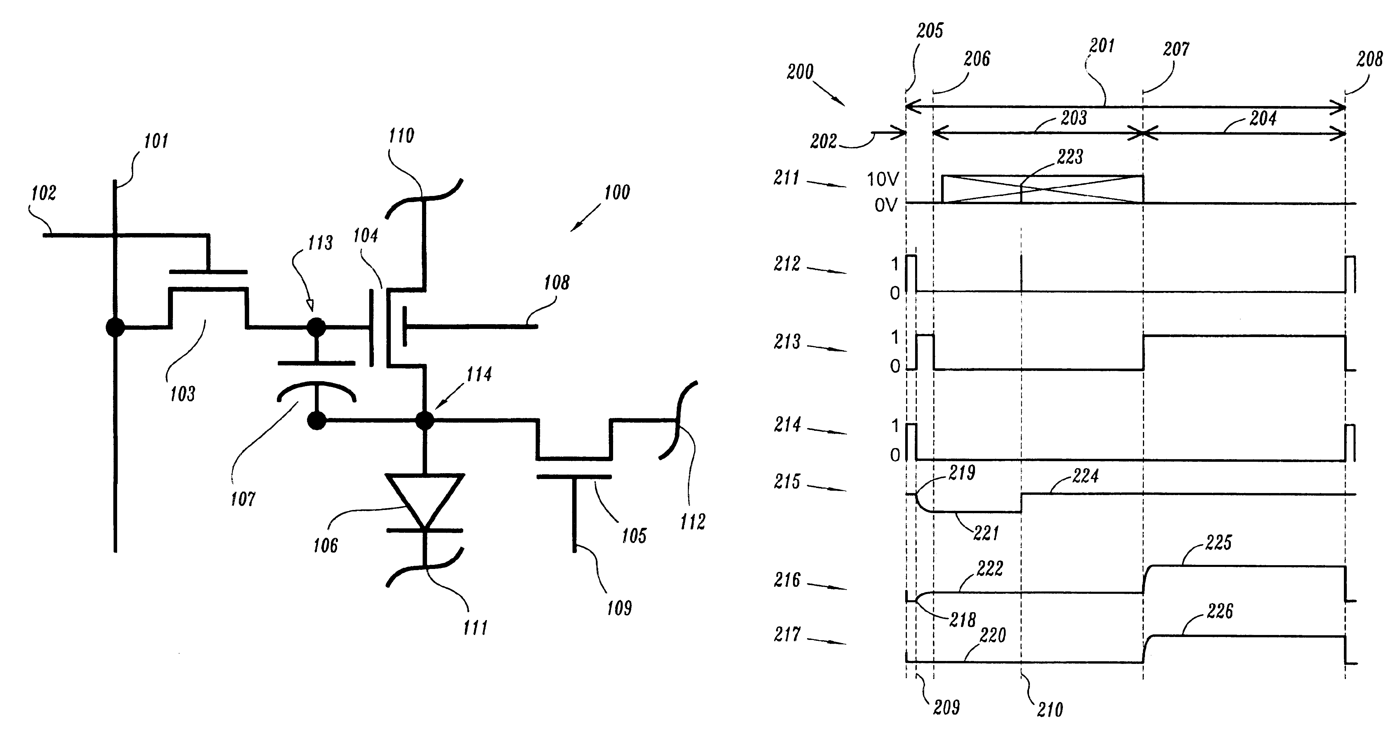
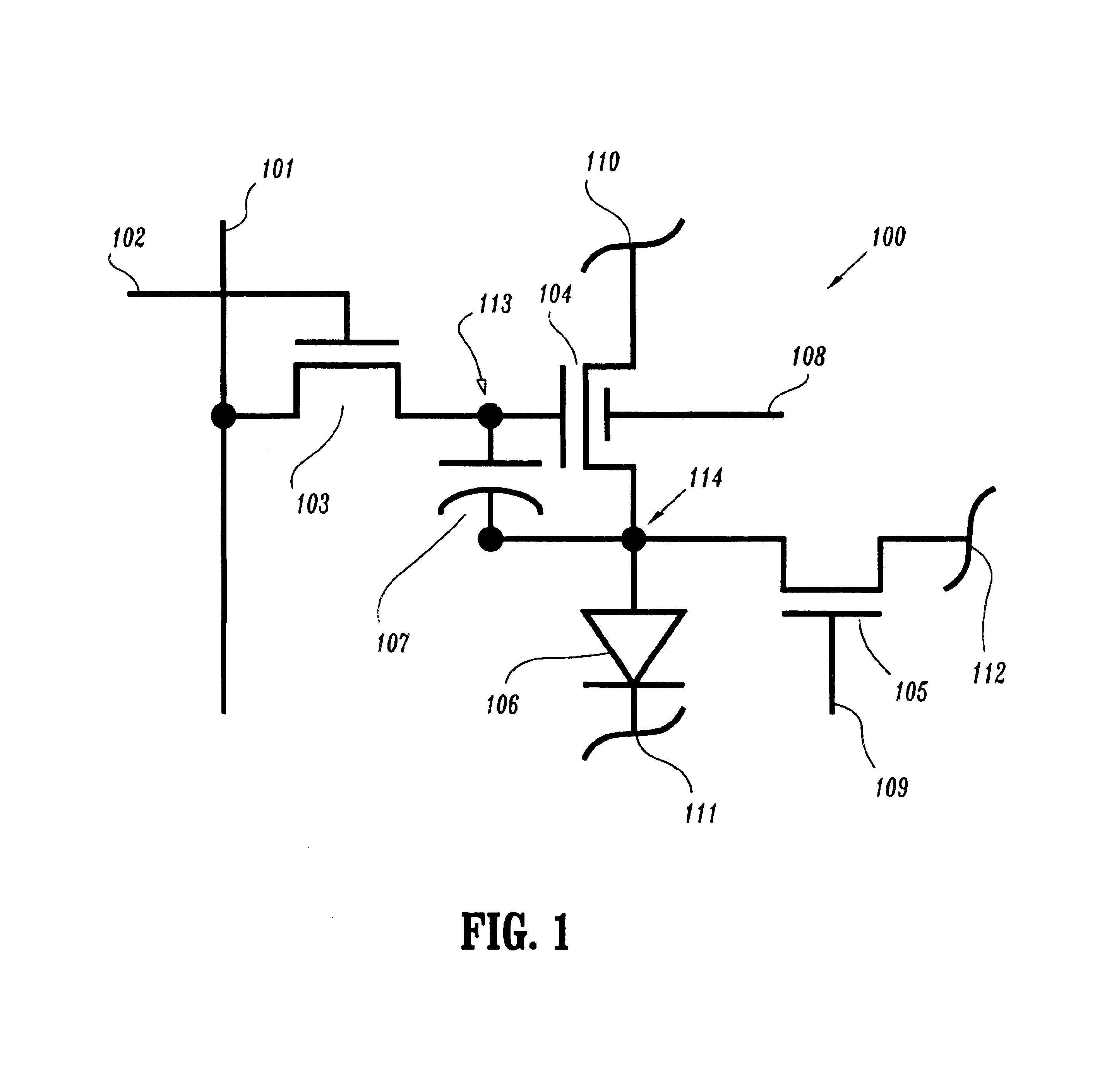
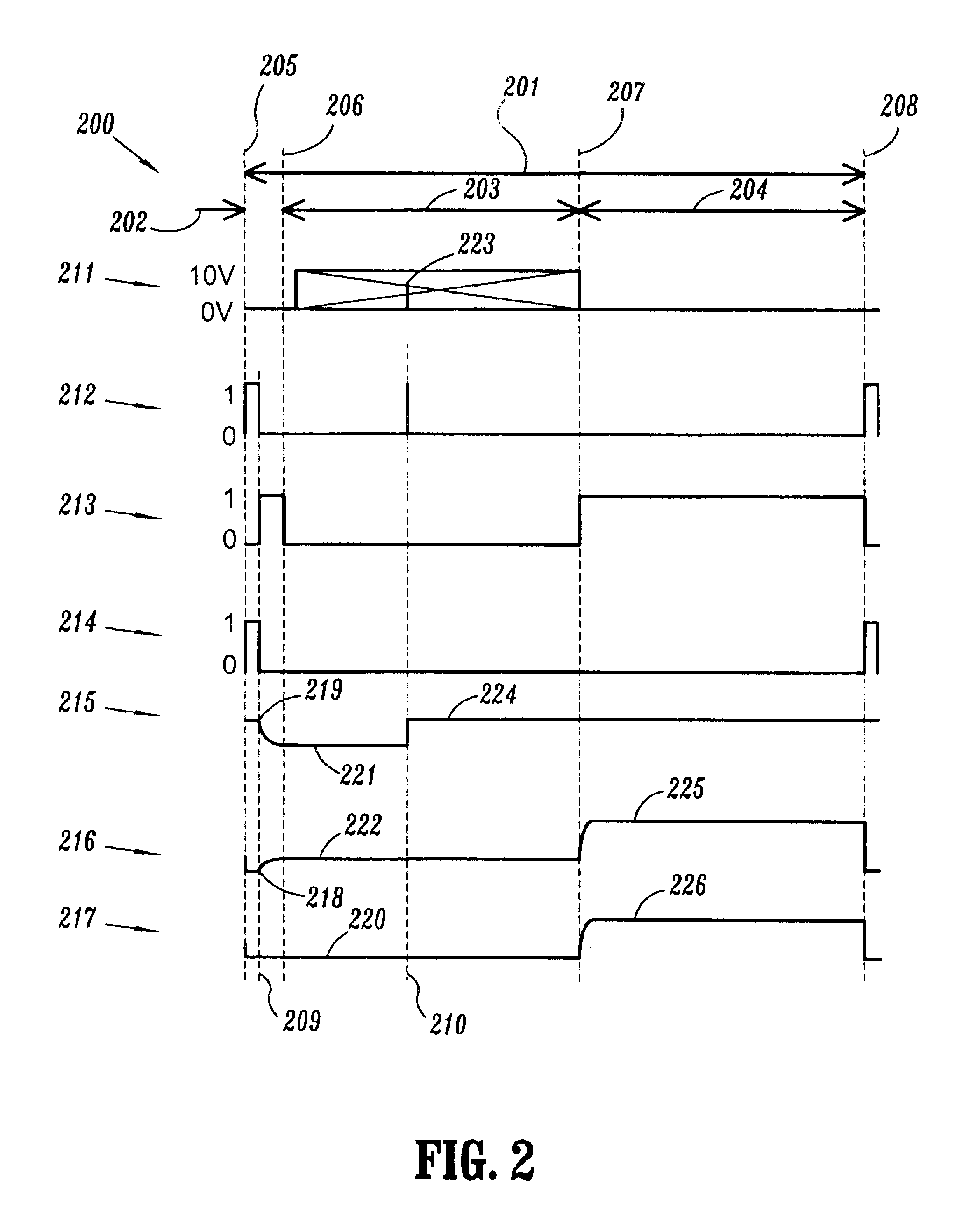
[0028]Referring now to the drawings, FIG. 1 shows an AMOLED pixel circuit suitable for fast threshold voltage (Vt) compensation without switching of the cathode voltage. The AMOLED pixel circuit 100 has four signal inputs 101, 102, 108 and 109; specifically, a data signal input 101 for carrying a column signal presenting analog voltage data i.e., converted image data, a gate signal input 102 for carrying a row addressing logic signal for writing data, an on / off signal input 108 for carrying a logic signal for allowing or preventing current flow by...


PUM


Abstract

An active matrix display includes a plurality of pixels arranged in an array, a first transistor and a second transistor associated with each pixel, the first and second transistors positioned within the array for controlling current flow through each pixel, a light emitting diode associated with each pixel; and a storage capacitor associated with each pixel, wherein, during a time period for establishment of a threshold voltage on the storage capacitor for the first transistor, a voltage equal to the sum of the threshold voltage and a voltage for compensating for turnoff of the second transistor is established on the storage capacitor.

Description

BACKGROUND OF THE INVENTION[0001]1. Field of the Invention[0002]The present invention relates to the formation of a uniform, light emitting, active matrix display and, more particularly, to an active-matrix light emitting display utilizing a less time consuming Vt compensation method that does not require switching of the OLED cathode voltage.[0003]2. Description of the Related Art[0004]Displays for computer and video devices are well-known in the art and may consist of, for example, liquid crystal or light emitting diodes (LEDs). The displays may consist of a number of display elements or pixels arranged in rows and columns to form a matrix on glass. In a passive matrix, signals are applied to a row line and a column line to illuminate a pixel formed at the intersection of the row and column line. In an active matrix, pixels formed at the intersection of row and column lines may consist of an organic LED (OLED), for example, connected to at least one thin-film transistor (TFT). Som...

Claims


Application Information

Patent Timeline
Patent Type & Authority Patents(United States)
IPC IPC(8): G09G3/10G09G3/32
CPCG09G3/3233G09G2300/0819G09G2300/0842G09G2330/06G09G2310/0251G09G2310/0254G09G2320/043G09G2300/0866
Inventor LIBSCH, FRANK ROBERTSANFORD, JAMES LAWRENCE
Owner TWITTER INC
Learn More