Drive circuit, electro-optical device and driving method thereof

a technology of electrooptical devices and drive circuits, applied in the direction of instruments, static indicating devices, etc., can solve the problems of increasing wasteful consumption of current, difficulty in providing a panel with low power consumption, and difficulty in realizing multicolor displays and/or motion picture displays

Inactive Publication Date: 2006-04-25
SEIKO EPSON CORP
View PDF11 Cites 24 Cited by
  • Summary
  • Abstract
  • Description
  • Claims
  • Application Information

AI Technical Summary

Benefits of technology

[0011]In the present invention, the first, second, and third switching signals for demultiplexing, which control turning the first, second and third switching elements on and off are produced. The overlapped period is during the periods of activating the first, second and third switching signals for demultiplexing (the period of activating at least two switching signals together). Hence, according to the present invention, it is possible to apply voltage (electric charging or discharging) to each of the pixels (pixel electrodes) for the first, second, and third color components connected to the first, second, and third switching elements for demultiplexing by using such overlapped period, enabling drift of data line voltage (pixel electrode voltage) to be minimized thereby.
[0016]Hence, drift of data line voltage (pixel electrode voltage) can be suppressed so as to set the data line voltage as a desirable voltage during a short time period.
[0024]Thus, it is possible to lower the output impedance of the reference-voltage output terminals so as to make it easy to set the data line voltage to a desirable voltage.
[0026]Hence, it is possible to lower the output impedance of the N reference voltage output terminals by using impedance conversion function of the M impedance conversion circuits.
[0028]Thus, it is possible to lower the output impedance of the reference voltage terminals while decreasing current flowing constantly in the ladder resistor.
[0032]Hence, it is possible to set the overlapped period easily during periods of activating the first, second, and third signals for demultiplexing.

Problems solved by technology

A simple matrix system has the advantage of providing a panel with lower power consumption but the disadvantage of difficulty in realizing a multicolor display and / or motion picture display.
On the other hand, an active matrix system has the advantage of ease in realizing a multicolor display and / or motion picture display but the disadvantage of difficulty in providing a panel with low power consumption.
However, when an operational amplifier is installed in an output circuit, there is a problem of increasing wastefully consumed current, namely large consumption of current.
Therefore, when power consumption of each operational amplifier increases, power consumption of data line drive circuits is increased by the number of these operational amplifiers, which adds to the problem of excess power consumption.

Method used


Image

  • Drive circuit, electro-optical device and driving method thereof
  • Drive circuit, electro-optical device and driving method thereof
  • Drive circuit, electro-optical device and driving method thereof

Examples


Embodiment Construction

[0062]A present embodiment is described in detail hereafter referring to drawings.

[0063]The present embodiments explained hereafter do not limit the spirit of the present invention described in the scope of the claims. In addition, all of constituents explained in the present embodiments may not be required as indispensable elements of the present invention.

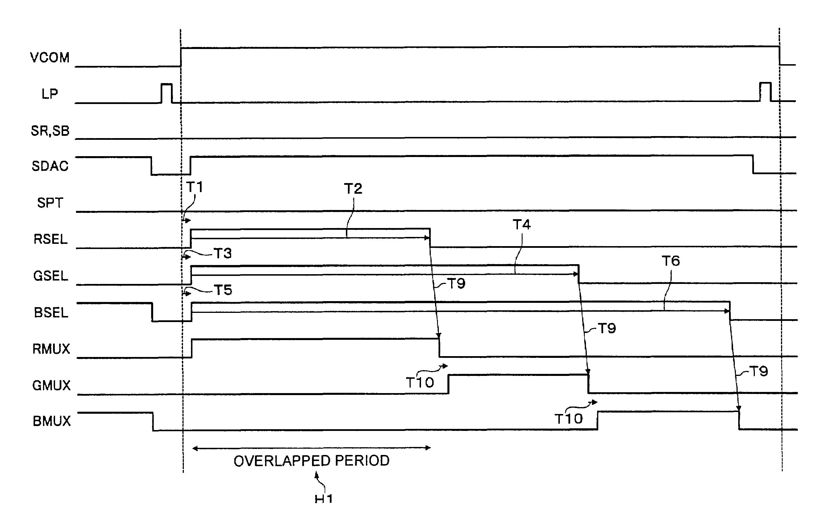
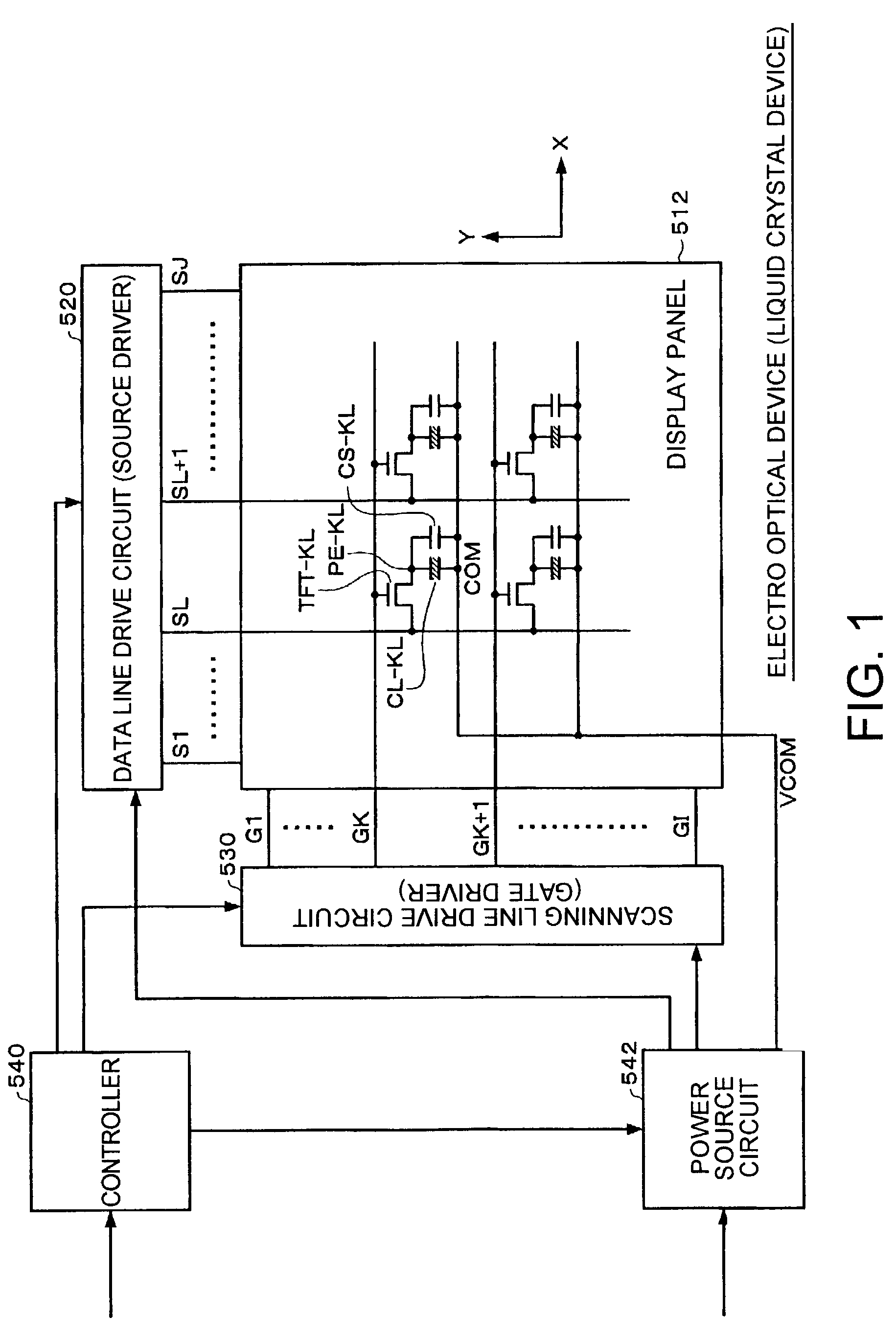
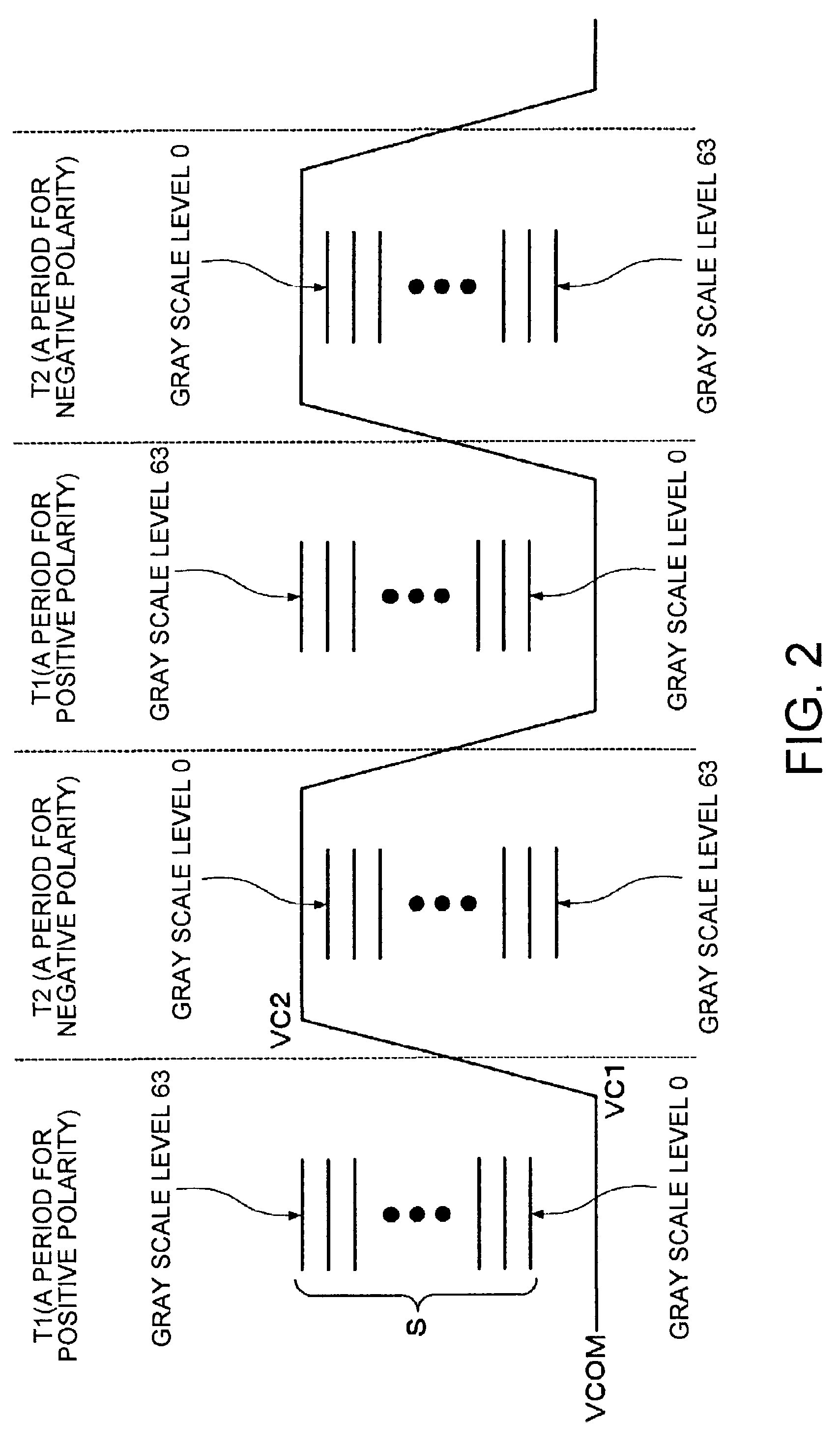
[0064]FIG. 1 shows an example of an electro-optical device of the present embodiment (e.g. a liquid crystal device).

[0065]This electro-optical device includes a display panel 512, such as a Liquid Crystal Display (LCD) panel, a data line drive circuit 520 (e.g. a source driver), a scanning line drive circuit 530 (e.g. a gate driver), a controller 540, and a power supply circuit 542. It is not necessary to include all these circuit blocks in an electro-optical device, and some of them may be omitted in a particular device.

[0066]The display panel 512 (electro-optical panel) includes plural scanning lines (gate lines), plural data l...


PUM


Abstract

A drive circuit is provided that can drive a display panel with low power consumption, and an electro optical device including the drive circuit and its drive method are included. Switching signals RSEL, GSEL, and BSEL for demultiplexing are produced so as to control turning switching elements DSWR, DSWG, and DSWB for demultiplexing on and off, which separate data signal where R, G, and B are multiplexed and transmitted. An overlapped period, for periods of activating RSEL, GSEL, and BSEL is set between the timing of changing polarity of common voltage and the timing of assuring writing data signal to a pixel electrode. A drive circuit includes a reference voltage production circuit and a digital to analog conversion circuit and an output circuit, which outputs a programmed voltage (a reference voltage having the same phase as the common voltage) during the overlapped period. The first reference voltage production circuit includes plurality of operational amplifiers and the first and second voltage division circuits.

Description

BACKGROUND OF THE INVENTION[0001]1. Field of the Invention[0002]The present invention relates to a drive circuit, an electro-optical device and a drive method.[0003]2. Description of the Related Art[0004]Conventionally, it is well known to use a liquid crystal panel using a simple matrix system or a liquid crystal panel using an active matrix system with thin film transistors (TFT) as a liquid crystal panel used for an electronic device such as a mobile phone.[0005]A simple matrix system has the advantage of providing a panel with lower power consumption but the disadvantage of difficulty in realizing a multicolor display and / or motion picture display. On the other hand, an active matrix system has the advantage of ease in realizing a multicolor display and / or motion picture display but the disadvantage of difficulty in providing a panel with low power consumption.[0006]Recently, in the area of mobile type electronic equipment such as mobile phones, demand has increased for a multic...

Claims


Application Information

Patent Timeline
IPC IPC(8): G09G3/36G02F1/133G09G3/20
CPCG09G3/3688G09G2330/021G09G2310/0297G09G2310/027G09G3/36
Inventor MAKI, KATSUHIKO
Owner SEIKO EPSON CORP
Why Eureka
Try Eureka