
Dual-type organic electroluminescence display and manufacturing method thereof

Active Publication Date: 2006-04-25
SAMSUNG DISPLAY CO LTD
View PDF10 Cites 20 Cited by
  • Summary
  • Abstract
  • Description
  • Claims
  • Application Information

AI Technical Summary

Benefits of technology

[0032]In still another aspect of the present invention, there is provided a method of manufacturing a dual-type organic EL display comprising preparing a main organic EL device by forming main substrate scan lines, a main substrate insulating layer, a main substrate organic layer, and main substrate data lines crossing the main substrate scan lines on a transparent main substrate, preparing a sub organic EL device by forming sub substrate scan lines, a sub substrate insulating layer, a sub substrate organic layer, and sub substrate data lines crossing th

Problems solved by technology

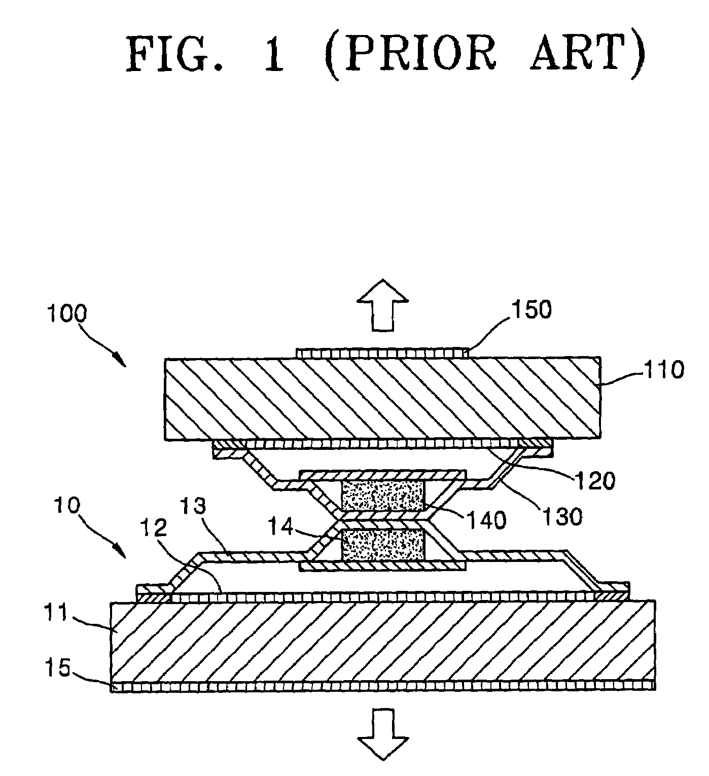
First, the caps 13 and 130, incorporating the respective moisture absorbents 14 and 140, are installed at a connected portion of the main organic EL device 10 and the sub organic EL device 100. The heights of the caps 13 and 130 are combined, resulting in an increase in the overall thickness of the dual-type organic EL display. Therefore, since there is a limitation in thinning, satisfactorily lightweight, miniaturized electronic devices cannot be obtained

Method used


Image

  • Dual-type organic electroluminescence display and manufacturing method thereof
  • Dual-type organic electroluminescence display and manufacturing method thereof
  • Dual-type organic electroluminescence display and manufacturing method thereof

Examples


Example

[0048]Reference will now be made in detail to the embodiments of the present invention, examples of which are illustrated in the accompanying drawings, wherein like reference numerals refer to the like elements throughout. The embodiments are described below to explain the present invention by referring to the figures.

[0049]FIG. 4 is a cross-sectional view of a dual-type organic EL display according to an embodiment of the present invention.

[0050]Referring to FIG. 4, the dual-type organic EL display includes a main organic EL device 40 and a sub organic EL device 400 connected to the main organic EL device 40, so display images are projected on two displays as indicated by the arrows.

[0051]A transparent main substrate 41 is provided in the main organic EL device 40, and a main substrate organic light-emitting portion 42 is formed on the main substrate 41.

[0052]The main substrate organic light-emitting portion 42 includes main substrate scan lines as first electrode lines, a main sub...


PUM


Abstract

A dual-type organic EL display including: a main organic EL device including a main substrate, strip-shaped main substrate scan lines, a main substrate organic light-emitting portion, and main substrate data lines formed on the main substrate; a sub organic EL device opposite to and facing the main organic EL device, including a sub substrate, strip-shaped sub substrate scan lines, a sub substrate organic light-emitting portion, and sub substrate data lines formed on the sub substrate; a sealant including a conductive spacer, sealing the main and sub substrates and hermetically sealing the main and sub substrate organic light-emitting portions in a state in which the main and sub organic El devices face each other; and at least one flexible printed cable (FPC) formed on the main or sub substrate and connected to electrode lines of the main and/or sub substrates.

Description

CROSS-REFERENCE TO RELATED APPLICATIONS[0001]This application claims the benefit of Korean Patent Application No. 2002-57389, filed on Sep. 19, 2002, in the Korean Intellectual Property Office, the disclosure of which is incorporated herein reference.BACKGROUND OF THE INVENTION[0002]1. Field of the Invention[0003]The present invention relates to a dual-type organic electroluminescence (EL) display and a manufacturing method thereof, and, more particularly, to a dual-type organic electroluminescence display having an improved connection structure of a flexible printed cable electrically connected to terminals provided at main and sub organic EL displays and an improved driving method, and a manufacturing method thereof.[0004]2. Description of the Related Art[0005]In general, organic EL displays are spontaneous light-emitting display devices which emit light through electrical excitation of fluorescent organic compounds, and provide various advantages including a low drive voltage and...

Claims


Application Information

Patent Timeline
IPC IPC(8): H01J1/62H05B33/10G09F9/00G09F9/40H01L27/32H01L51/00H01L51/40H01L51/50H01L51/56H05B33/00H05B33/14H05B33/26
CPCH01L25/048H01L27/3288H01L51/5246H05K1/189H01L27/3286H01L51/0024H05K2201/10446H01L2924/0002H01L51/56H05K2201/10128H01L2924/00H10K59/90H10K59/176H10K59/179H10K71/50H10K50/8426H10K71/00H05B33/00
Inventor KIM, TAE SEUNG
Owner SAMSUNG DISPLAY CO LTD
Learn More