
Specification of the hierarchy, connectivity, and graphical representation of a circuit design

a circuit design and hierarchy technology, applied in the direction of static indicating devices, instruments, program control, etc., can solve the problems of large number of blocks, complex connections, overwhelming hand-made assembly,

Active Publication Date: 2006-02-21
XILINX INC
View PDF9 Cites 31 Cited by
  • Summary
  • Abstract
  • Description
  • Claims
  • Application Information

AI Technical Summary

Problems solved by technology

Often this approach suitable, but there are circumstances when this approach is not.
For example, designs sometimes contain thousands of blocks, and assembling by hand can be overwhelming.
Finally, there though the number of blocks is large and connections are intricate.

Method used


Image

  • Specification of the hierarchy, connectivity, and graphical representation of a circuit design
  • Specification of the hierarchy, connectivity, and graphical representation of a circuit design
  • Specification of the hierarchy, connectivity, and graphical representation of a circuit design

Examples


example 1

[0021]

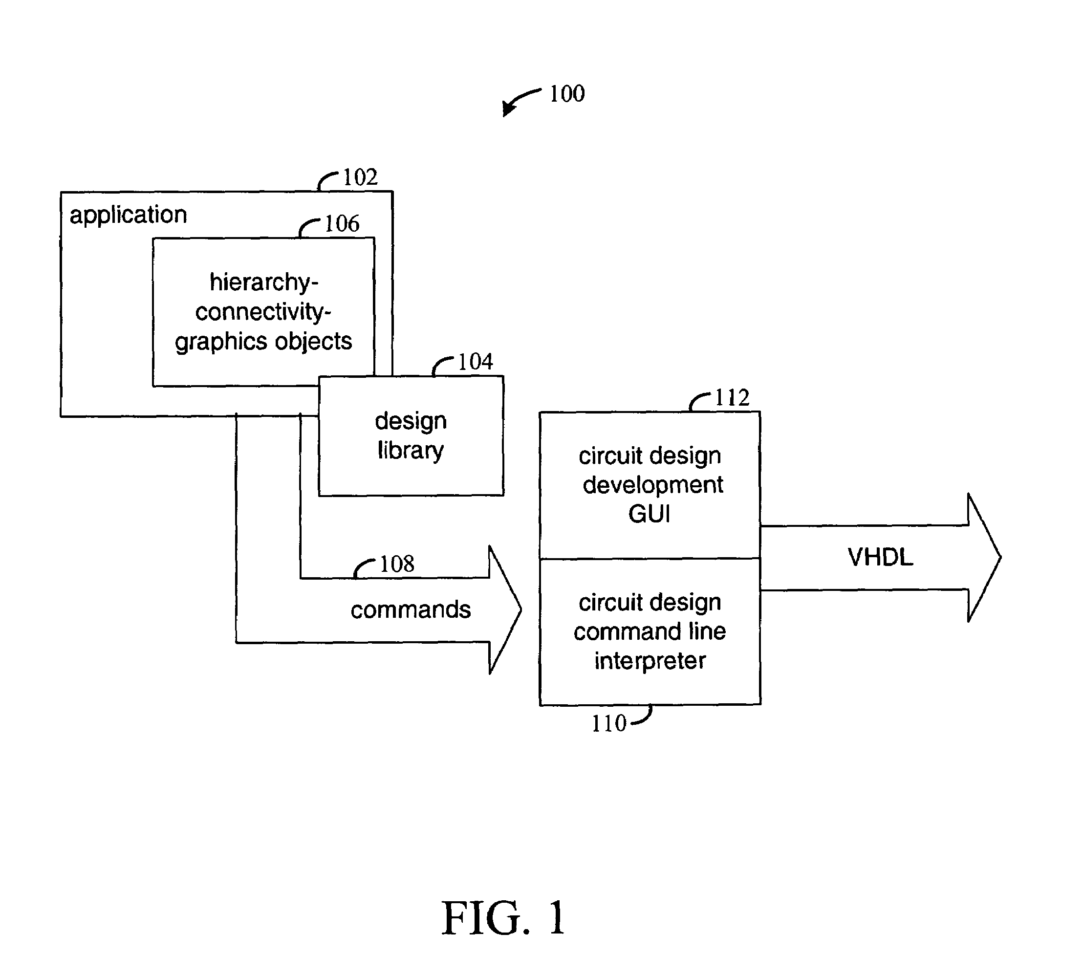
[0022]The first line declares Commutator to be a class that extends the Module class. An application built using design library 104 generally contains one or several such classes. Instances of these classes become blocks and levels of hierarchy when the design is realized. The lines,[0023]super(name, null, null, null);[0024]this.makeSchematicSheet( );

make the new object a top-level object (step 202). The lines also indicate that in Simulink the object is to be given its own schematic sheet. The next few lines,[0025]double w=100;[0026]double h=50;[0027]double [ ] nwc={0, 0,};[0028]double [ ] sec={4*w, (2*n−1)*h,};[0029]Frame tf=new Frame(nwc, sec);[0030]this.setLowerFrame(tf);

build the lower frame for the top level, i.e., the frame that holds the body of the commutator (step 202). The frame is defined to be 4*w units wide and (2n−1) units high. The statements w=100 and h=50 denote, respectively, the width and height in pixels of a single block. Defining the size in this way mak...


PUM


Abstract

Method and apparatus for creating a circuit design. An object-oriented program instantiates a plurality of objects that model a circuit design. The objects have hierarchy attributes, connectivity attributes, and display attributes that describe a plurality of modules. The hierarchy attributes define parent-child relationships between modules, the connectivity attributes define input-output connections between modules, and the display attributes define a layout of the modules for viewing. Each of the objects has an associated method for generating a design specification in a selected format. When the program is executed, the design specification is generated from the set of objects. Depending on the capabilities of the available tools, the modules and logic elements are displayed in accordance with the display attributes either from the object-oriented program or from the design specification.

Description

FIELD OF THE INVENTION[0001]The present invention relates to tools for developing circuit designs.BACKGROUND[0002]There are many software tools in which electronic designs can be built, debugged, and translated into hardware for field programmable gate arrays(FPGAs). Some, such as Altera's DSP Builder, Cadence's Signal Processing Worksystem, and Xilinx's System Generator for DSP, are high-level, abstract, visual environments. In these tools, flexible signal types, polymorphic blocks, automatic faithful generation of hardware, and straightforward analysis of results reduce the distance between algorithm and implementation, simplifying the job of the designer.[0003]Ordinarily in such tools, a user assembles a design by hand, dragging blocks and connecting them with a mouse. Often this approach suitable, but there are circumstances when this approach is not. For example, designs sometimes contain thousands of blocks, and assembling by hand can be overwhelming. For some designs the coll...

Claims


Application Information

Patent Timeline
Patent Type & Authority Patents(United States)
IPC IPC(8): G06F17/50
CPCG06F17/5045G06F30/30
Inventor STROOMER, JEFFREY D.MILNE, ROGER B.BALLAGH, JONATHAN B.MA, HAIBINGHWANG, L. JAMESSHIRAZI, NABEEL
Owner XILINX INC
Learn More