
Sensitive test structure for assessing pattern anomalies

a sensitive test and pattern anomaly technology, applied in the field of semiconductor technology, can solve the problems of adversely affecting the performance and reliability of the resultant chip, and compromise the structure performance, so as to facilitate the identification of process drift, facilitate the determination of process drift, and facilitate the determination of semiconductor fabrication process dri

Inactive Publication Date: 2005-11-22
TEXAS INSTR INC
View PDF7 Cites 91 Cited by
  • Summary
  • Abstract
  • Description
  • Claims
  • Application Information

AI Technical Summary

Benefits of technology

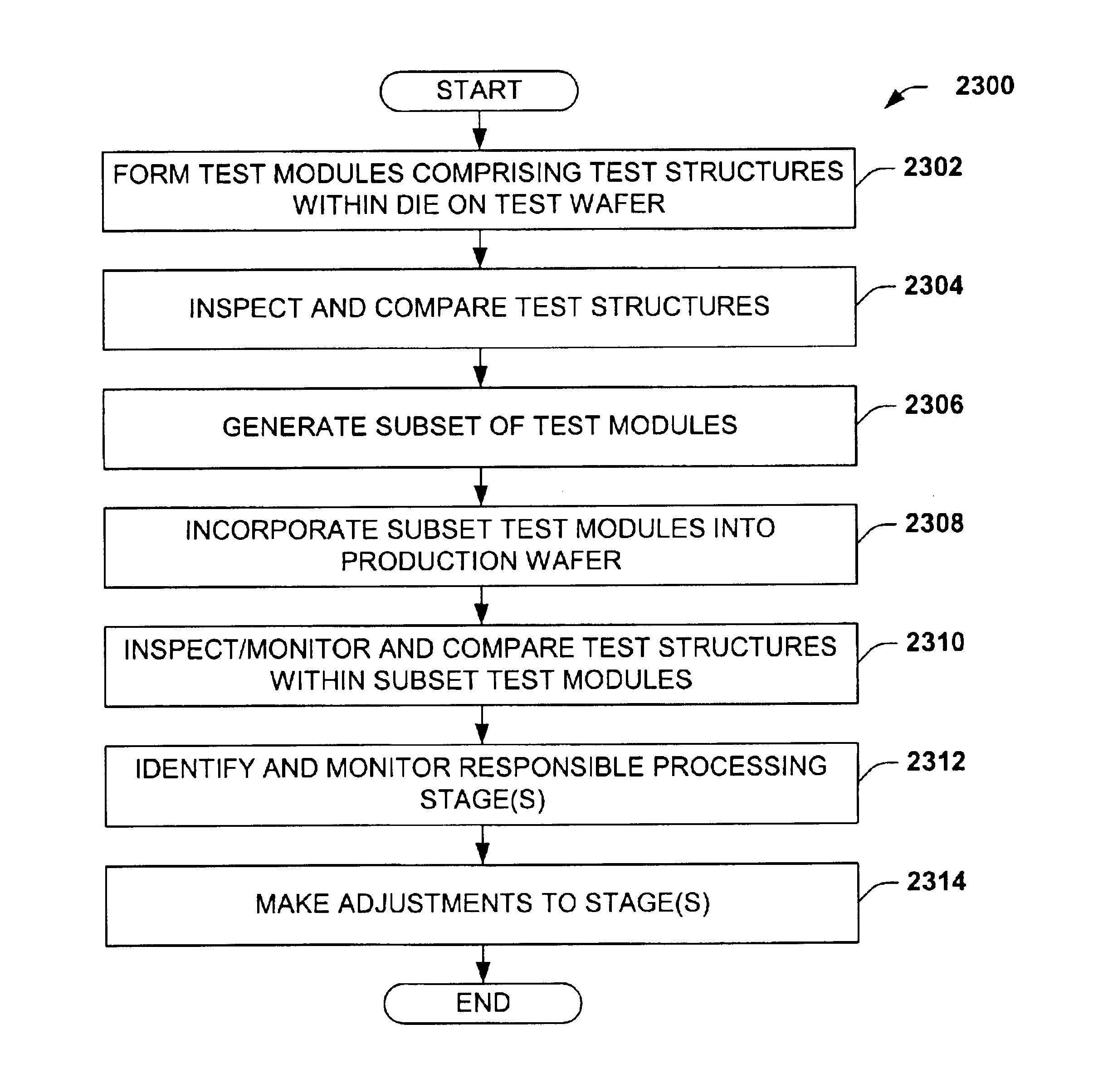
The present invention relates to a method and apparatus for identifying process drift in semiconductor fabrication processes. More specifically, it involves creating subsets of testing materials (test modules) containing identical test structures that show sensitivity to process drift or abnormal processing conditions. These tests are placed on separate dies on a test wafer and results from these tests are used to compare data collected from various parts of the manufacturing process. By analyzing this data, patterns indicating potential issues with the overall process can be identified and addressed before causing significant damage to the finished product.

Problems solved by technology

The technical problem addressed in this patent text is how to improve the production efficiency and reduce costs associated with making highly dense electronics while maintaining their quality and reliability. This involves reducing the space requirements for components within the device, improving the accuracy and precision of component formation, and optimizing the overall manufacturing process.

Method used


Image

  • Sensitive test structure for assessing pattern anomalies
  • Sensitive test structure for assessing pattern anomalies
  • Sensitive test structure for assessing pattern anomalies

Examples


Embodiment Construction

[0035]One or more aspects of the present invention are described with reference to the drawings, wherein like reference numerals are generally utilized to refer to like elements throughout, and wherein the various structures are not necessarily drawn to scale. In the following description, for purposes of explanation, numerous specific details are set forth in order to provide a thorough understanding of one or more aspects of the present invention. It may be evident, however, that one or more aspects of the present invention may be practiced with a lesser degree of these specific details. In other instances, structures and devices are shown in block diagram form in order to facilitate describing one or more aspects of the present invention.

[0036]It is to be appreciated that various aspects of the present invention may employ technologies associated with facilitating unconstrained optimization and / or minimization of error costs. Thus, non-linear training systems / methodologies (e.g.,...


PUM


Abstract

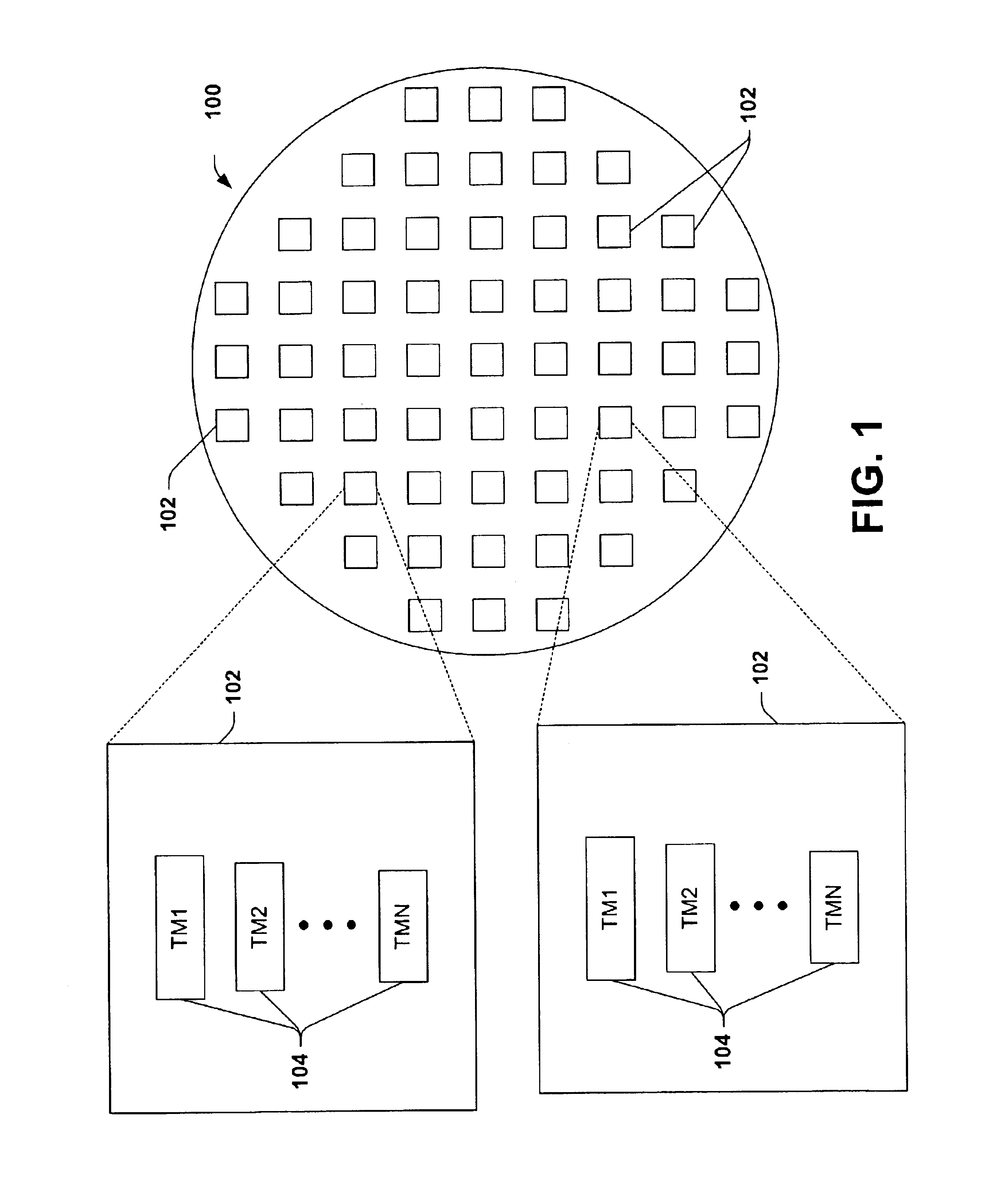
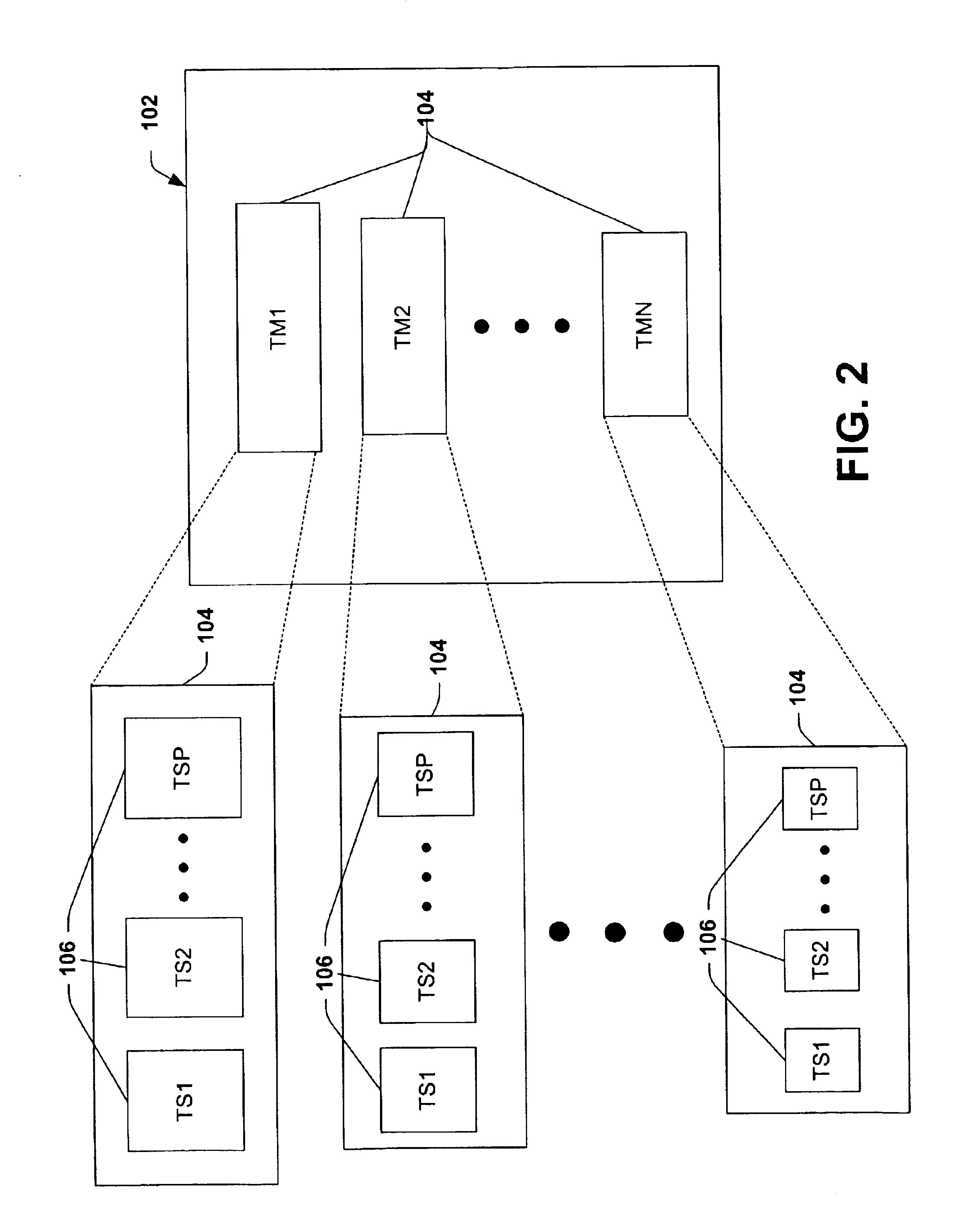
A subset test module and associated methodology for utilizing the same are disclosed that facilitate identification of process drift in semiconductor fabrication processing. A test wafer having a plurality of die formed thereon has a plurality of test modules formed within the die. The plurality of test modules are substantially the same from die to die, and the respective modules similarly include a plurality of test structures that are substantially the same from module to module. Corresponding test structures within respective modules on different die are inspected and compared to one another to find structures that are sensitive to process drift. One or more structures that experience differences from module to module on different die are utilized to develop one or more test modules that can be selectively located within production wafers and monitored to determine whether process drift and/or one or more other aberrant processing conditions are occurring.

Description


Claims


Application Information

Patent Timeline
Owner TEXAS INSTR INC
Learn More