Operation method for non-volatile memory
- Summary
- Abstract
- Description
- Claims
- Application Information
AI Technical Summary
Benefits of technology
Problems solved by technology
Method used
Image
Examples
Embodiment Construction
[0018]Embodiments of the present invention are now being described with reference to the accompanying drawings.
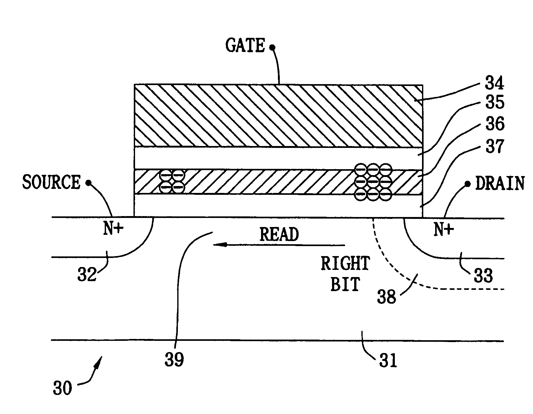
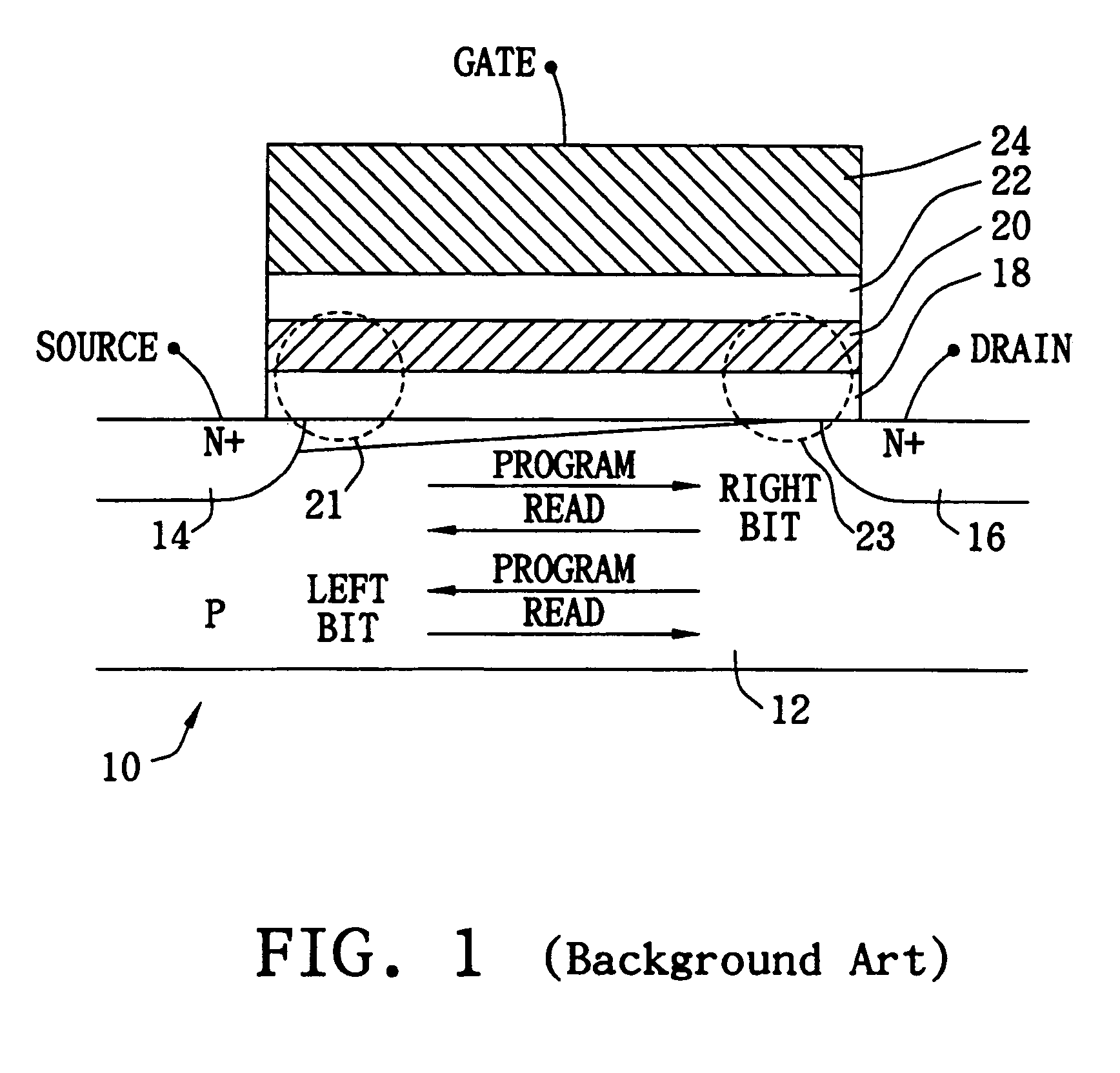
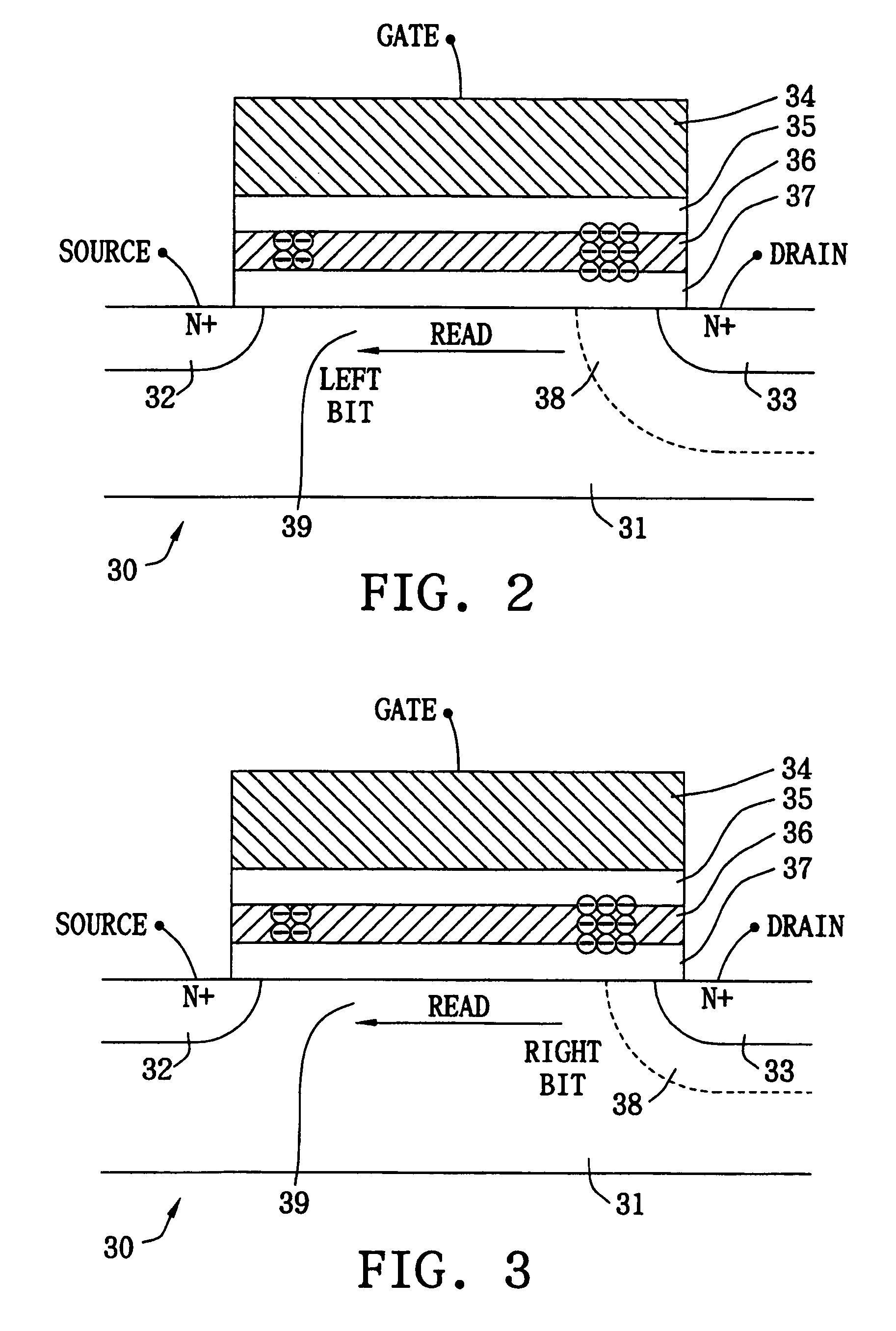
[0019]Referring to FIG. 2, a non-volatile memory cell 30 of NMOS type is built up on a silicon substrate 31, in which a source 32 and a drain 33 are formed, and a gate 34, an first dielectric layer 35, a charge trapping layer 36 and a second dielectric layer 37 are formed thereon. The charge trapping layer 36 may be composed of silicon nitride, and the first and second dielectric layers 35, 37 may be made of silicon dioxide. The non-volatile memory cell 30 can be programmed by the way of conventional art, for example, the drain 33 and gate 34 are respectively applied by voltages VD and VG, e.g., larger than or equal to 5V and 5V, respectively, so as to program the left bit near the source 32 to a voltage of 3.5V. The right bit near the drain 33 can be programmed to a voltage of 5.5V by applying voltages larger than 6V to the drain 33 and 5V to the gate 34, respectively. The...
PUM
 Abstract
Description
Claims
Application Information
 - R&D
- Intellectual Property
- Life Sciences
- Materials
- Tech Scout
- Unparalleled Data Quality
- Higher Quality Content
- 60% Fewer Hallucinations
Browse by: Latest US Patents, China's latest patents, Technical Efficacy Thesaurus, Application Domain, Technology Topic, Popular Technical Reports.
© 2025 PatSnap. All rights reserved.Legal|Privacy policy|Modern Slavery Act Transparency Statement|Sitemap|About US| Contact US: help@patsnap.com


