Interpolation delay cell for 2ps resolution jitter injector in optical link transceiver

a delay cell and injector technology, applied in the field of delay circuits, can solve the problems of limited timing resolution, inability to adapt to the changing environment of the amplifier, and the inherent limitations of the delay cell, and achieve the effects of reducing the tuning range and timing resolution of the jitter noise generator, and reducing the interference of the delay cell

Inactive Publication Date: 2005-10-25
INTEL CORP
View PDF6 Cites 11 Cited by
  • Summary
  • Abstract
  • Description
  • Claims
  • Application Information

AI Technical Summary

Problems solved by technology

More specifically, during normal operating conditions an optical receiver is expected to receive data which is corrupted by noise.
These capabilities are largely constrained by the inherent limitations of their internal delays cells.
The FIG. 1 delay cell has proven to significantly limit the tuning range and timing resolution of jitter noise generators, as well as other circuits.
Timing resolution is limited, for example, by the minimum delay of the cell.
This, in turn, limits ability of the generator to evaluate the performance of clock and data recovery circuits, which are vital to ensuring proper operation of high-speed communication and signaling systems.
Also, because the delay cell accepts only one input, it cannot perform phase interpolation for its input signal that may be desirable for evaluating performance of the receiver.

Method used


Image

  • Interpolation delay cell for 2ps resolution jitter injector in optical link transceiver
  • Interpolation delay cell for 2ps resolution jitter injector in optical link transceiver
  • Interpolation delay cell for 2ps resolution jitter injector in optical link transceiver

Examples


Embodiment Construction

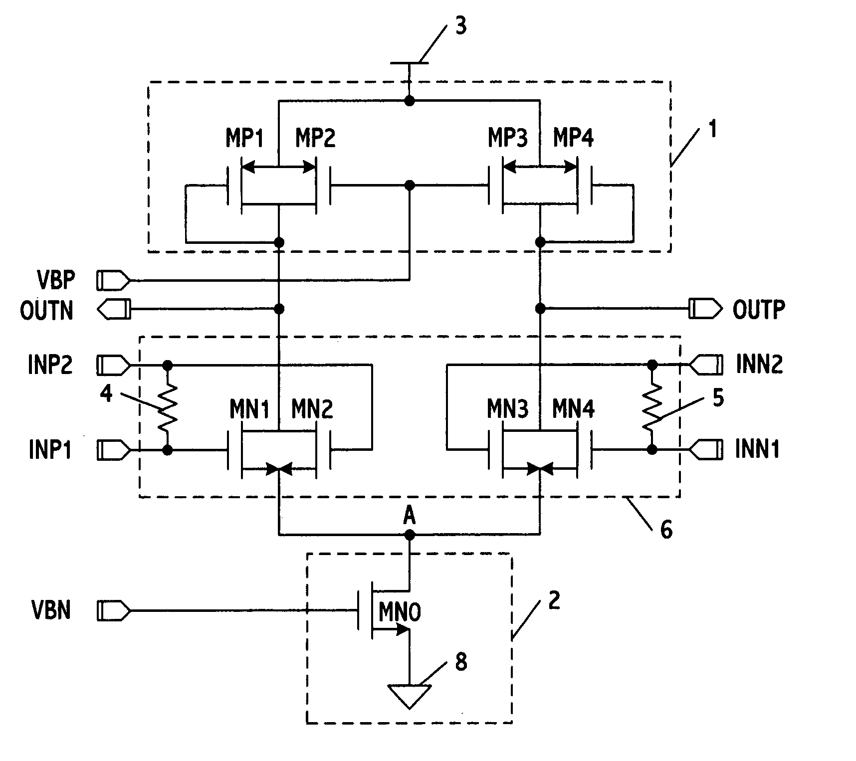
[0013]FIG. 2 shows a delay cell in accordance with a first embodiment of the present invention. The delay cell includes dual coupled differential input lines connected between a load 1 and a current source 2, a line 3 which functions as a power supply for the delay cell, and a differential output line coupled between the differential input lines and the load. These elements are preferably implemented using CMOS technology as described in greater detail below. VBP serves as a delay control line for the cell.

[0014]The load is preferably formed from a symmetrical arrangement of two pairs of coupled transistors. The first pair of transistors MP1 and MP2 have their sources and drains coupled together, and a gate of MP1 is connected to the common drain of MP1 and MP2. The second pair of transistors MP3 and MP4 are connected in a similar manner, i.e., the sources and drains of these transistors are connected and the gate of MP4 is connected to the common drain of MP3 and MP4. In this embod...


PUM


Abstract

An apparatus and method for generating signals with improved timing resolution includes a delay cell configured to receive dual coupled differential input signals. The delay cell performs an interpolation function which smooths state transitions or other discontinuities that result from timing or phase offsets between the input signals. The interpolation function is performed by resistors which couple respective components of the differential inputs prior to traversing delay paths. A delay cell of this type has high supply noise rejection and a low output swing range, thereby making it suitable for a number of applications. One application includes a jitter noise generator which uses the delay cell to achieve improved timing resolution and which is not limited by a minimum delay of the cell. Another application uses the delay cell to form a coupled delay line.

Description

FIELD[0001]This invention generally relates to delay circuits and their applications to programmable jitter injectors.BACKGROUND OF THE INVENTION[0002]High-speed communication systems use recovery circuits to regenerate clock and data signals from scrambled inputs that have been corrupted by jitter, inter symbol interference, and other forms of noise. In order to evaluate the performance of clock and data recovery circuits in an optical link receiver without any photonic devices or electro-optical conversion, a circuit known as jitter noise generator has been used.[0003]More specifically, during normal operating conditions an optical receiver is expected to receive data which is corrupted by noise. In order to evaluate its performance limitations, the receiver can be tested without connecting it to an optical link. A jitter noise generator is one type of testing device that can be used for this purpose. During a test, a jitter noise injector inputs noise into the receiver in order t...

Claims


Application Information

Patent Timeline
Patent Type & Authority Patents(United States)
IPC IPC(8): H03H11/26H03F1/26H03F3/45
CPCH03F1/26H03F3/45183H03F3/45475H03H11/265H03F2200/372
Inventor LEE, KYEHYUNGXU, JIANPINGPAILLET, FABRICEKARNIK, TANAY
Owner INTEL CORP
Why Eureka
Try Eureka