Eureka AIR delivers breakthrough ideas for toughest innovation challenges, trusted by R&D personnel around the world.

Chirped optical MEM device

a technology of optical mem devices and chirping, which is applied in the direction of optics, optical elements, instruments, etc., can solve the problems of affecting the quality of optical signals, and achieve the effect of improving alignmen

Inactive Publication Date: 2005-08-23
SILICON LIGHT MACHINES CORP
View PDF875 Cites 19 Cited by
  • Summary
  • Abstract
  • Description
  • Claims
  • Application Information

AI Technical Summary

Benefits of technology

[0005]According to embodiments of the present invention, a method of and apparatus for improving the alignment between chirped incident wavelengths of light and the center line of their respective pixels when the WDM signal is demultiplexed through a static grating demultiplexer is disclosed. The present invention is also a method of and apparatus for compensating for the variation of polarizat

Problems solved by technology

Variability in the characteristics of optical signals can be detrimental in applications where consistent optical signal characteristics are desired across the wavelength band and over time.

Method used


Image

  • Chirped optical MEM device
  • Chirped optical MEM device
  • Chirped optical MEM device

Examples


Embodiment Construction

[0022]Reference will now be made in detail to embodiments of the invention, examples of which are illustrated in the accompanying drawings.

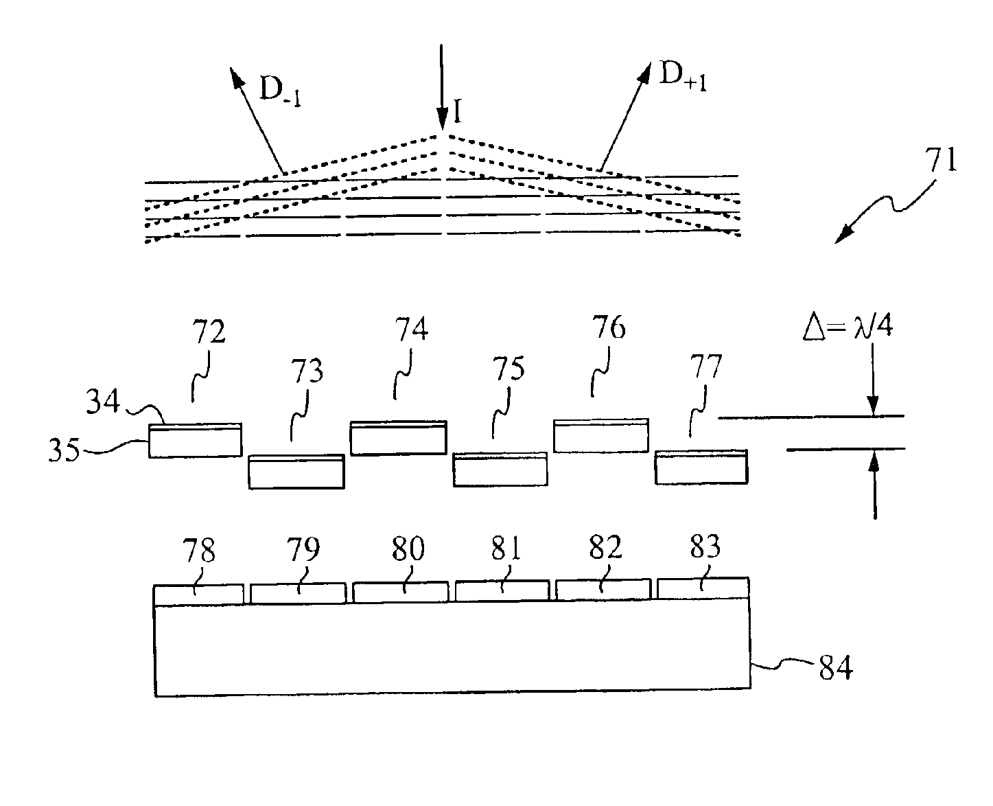
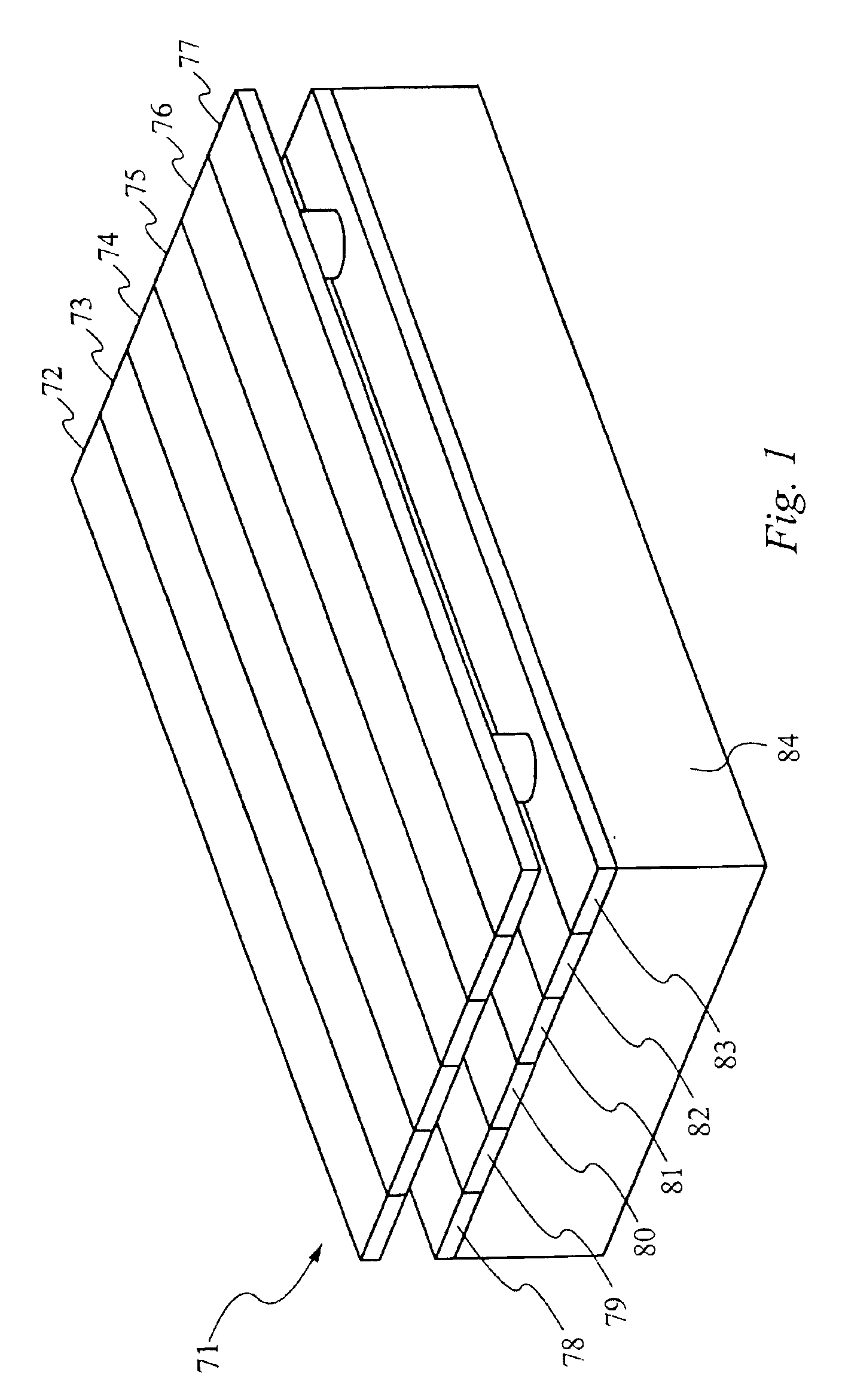
[0023]FIG. 1 is a perspective view of a grating light valve™ light modulator 71. Parallel ribbons 72-77 rest above a substrate 84 using any conventional technique. The substrate includes conductive members 78-83 which function to exert a field on their respective ribbons 72-77. A voltage potential formed between a ribbon 72-77 and its respective conductive member 78-83 exerts a force sufficient to deflect a ribbon 72-77.

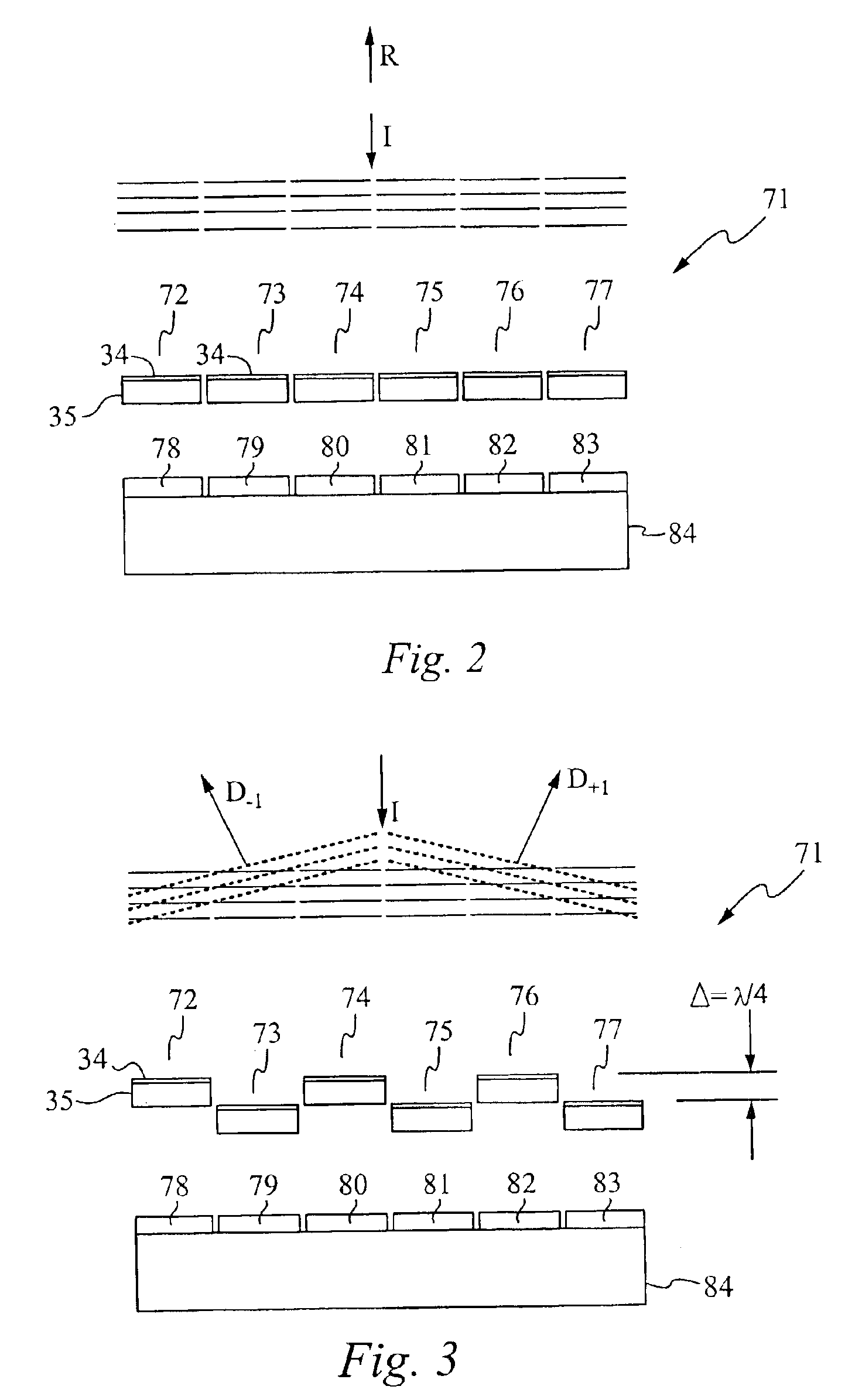
[0024]FIG. 2 illustrates a cross section side view of a grating light valve™ light modulator 71. In FIG. 2, the even ribbons 72, 74, 76 and odd ribbons 73, 75, 77 are at the same height above the substrate 84. Incident light I reflects substantially as a specular mirror when a grating light valve™ light modulator is configured as shown in FIG. 2. The ribbons are illustrated as comprising a reflective portion 34 and a resilient por...


PUM


Abstract

A light modulator comprises a series of ribbons divided by a series of gaps. Sequences of consecutive ribbons and gaps are grouped together to form a plurality of pixels that are configured to process a respective plurality of wavelengths. The spacing from center-line to center-line of adjacent pixels is progressively increased from a reference pixel to align component pixels with their assigned wavelengths. The widths of ribbons and gaps within a particular pixel affect the polarization dependent loss of a pixel, and affect the first order diffraction angle. Ribbon widths and gap widths within successive pixels are altered to normalize polarization dependent loss and first order diffraction angles against the values associated with a reference pixel.

Description

FIELD OF THE INVENTION[0001]The present invention relates to the field of grating light valves arranged in an array of pixels. More particularly, the present invention relates to chirping the widths of various grating light valve components in successive pixels to compensate for unwanted phenomena in a demultiplexed wavelength division multiplexed “WDM” signal.BACKGROUND OF THE INVENTION[0002]Optical MEM (micro-electro-mechanical) devices have applications in display, print, optical and electrical technologies. An optical MEM device, herein, is a device that is capable of constructively and destructively interfering with an incident light source to produce an optical signal or optical signals. Exemplary optical MEM devices, and methods for making the same, are disclosed in U.S. Pat. No. 5,311,360 entitled “METHOD AND APPARATUS FOR MODULATING A LIGHT BEAM,” U.S. Pat. No. 5,841,579 entitled “FLAT DIFFRACTION GRATING LIGHT VALVE” and U.S. Pat. No. 5,808,797 entitled “METHOD AND APPARAT...

Claims


Application Information

Patent Timeline
IPC IPC(8): G02B26/00G02B26/08
CPCG02B26/0808
Inventor MAHESHWARI, DINESHTRISNADI, JAHIACORRIGAN, ROBERT W.
Owner SILICON LIGHT MACHINES CORP
Why Eureka
Eureka Blog
Learn More