Optoelectric module for multi-fiber arrays
a multi-fiber array and optoelectric technology, applied in the field of optoelectric devices for use with multi-fiber arrays, can solve the problems of small form factor designs, increased space required, and prone to limi
- Summary
- Abstract
- Description
- Claims
- Application Information
AI Technical Summary
Benefits of technology
Problems solved by technology
Method used
Image

Examples
example
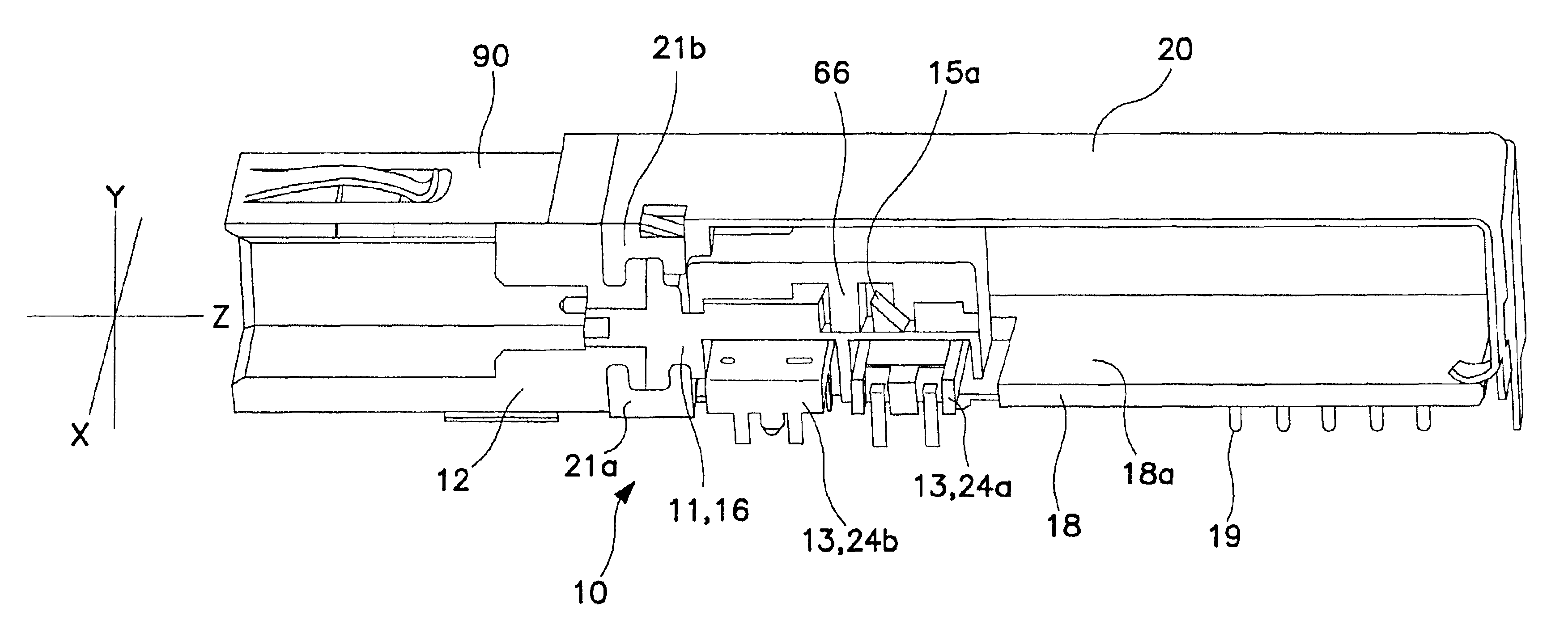
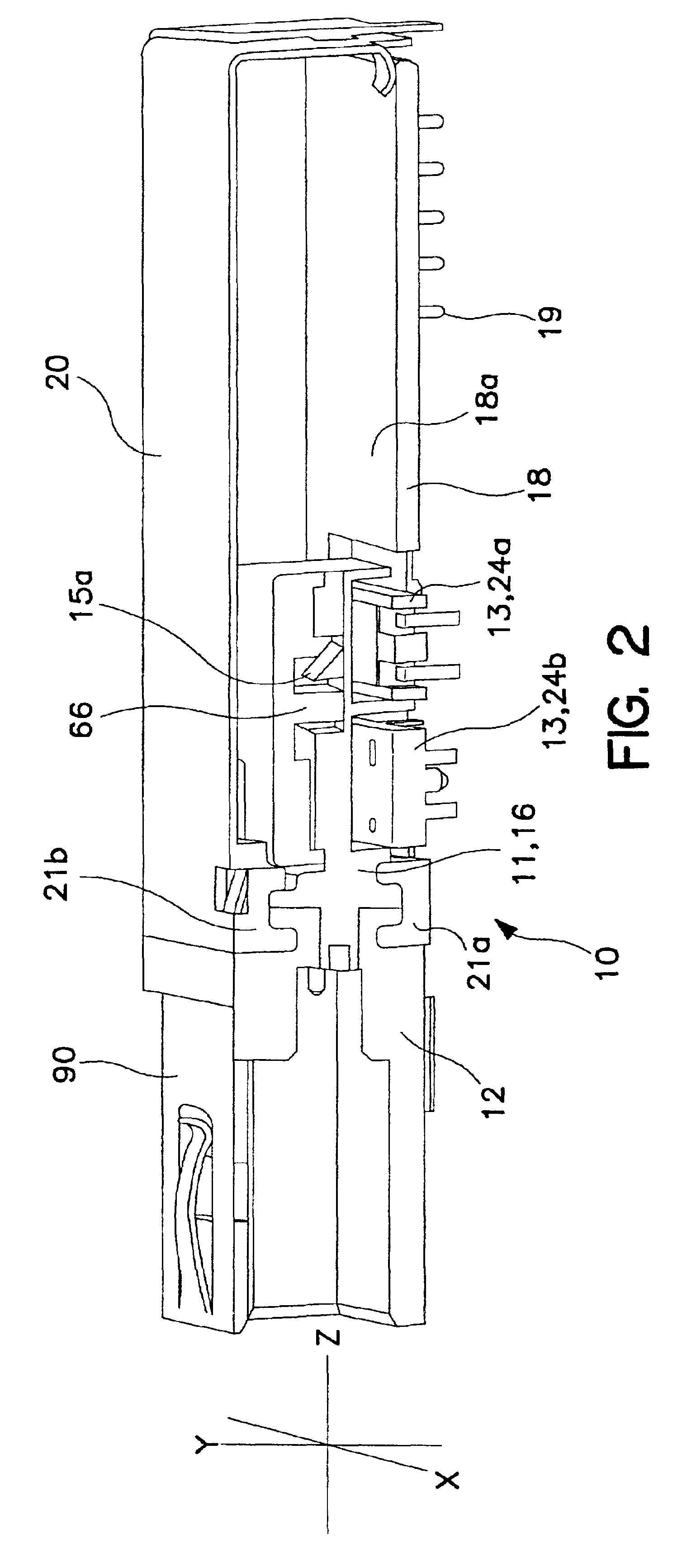
[0070]The optical block 16 of FIG. 6 and the optical paths it defines, including its feedback configuration, are described in particular detailed with respect to the ray tracing diagrams shown in FIGS. 7(a)-(c). It should be understood that optical block 16 and the optical paths defined therein are merely represented of the invention, and not exhaustive. For example, optical block 16 is used in a transceiver and defines two optical paths: one path couples optical signals from a fiber to a photodetector, while the other path couples optical signals from the OED to the fiber. Clearly, however, the present invention covers more than just two optical paths, and the optical paths can be used for propagating signals in either direction.
[0071]FIG. 7(a) shows the design concept of the transmitter. The light from a VCSEL on a lead frame 24a goes through a second lens 67a on its way to the coupled fiber. To accommodate the oxide VCSEL's large divergent angle, the optical lens 67a has a 1.4:1 ...
PUM
 Abstract
Description
Claims
Application Information
 - R&D
- Intellectual Property
- Life Sciences
- Materials
- Tech Scout
- Unparalleled Data Quality
- Higher Quality Content
- 60% Fewer Hallucinations
Browse by: Latest US Patents, China's latest patents, Technical Efficacy Thesaurus, Application Domain, Technology Topic, Popular Technical Reports.
© 2025 PatSnap. All rights reserved.Legal|Privacy policy|Modern Slavery Act Transparency Statement|Sitemap|About US| Contact US: help@patsnap.com