Electrically reconfigurable optical devices

Inactive Publication Date: 2005-06-07
INTELLECTUAL VENTURES I LLC
View PDF13 Cites 90 Cited by
  • Summary
  • Abstract
  • Description
  • Claims
  • Application Information

AI Technical Summary

Benefits of technology

[0023]The main purpose of the present invention is to produce a novel reconfigurable optical device, which is based on the use of electrically deformable viscoelastic layer in order to manipulate the light passing through said viscoelastic layer, but which is not limited to producing only sinusoidally varying grating structures. This innovation allowing to manipulate the viscoelastic layer in completely new ways broadens significantly the possibilities to use electrically controlled viscoelastic materials for optical switching applications.
[0025]In one specific embodiment of the invention, the electrode structure is arranged to form an electrically configurable blazed grating. A blazed grating can be used to diffract substantially all of the incident light in one direction or to one target (diffraction order) at a time, which provides the possibility to accomplish optical switching without significant loss of light. Thus, in this respect, the performance of a blazed grating is superior compared to a sinusoidal grating, which diffracts light intrinsically simultaneously at least in two different diffraction orders (directions).
[0027]The devices according to the invention are significantly more advantageous than prior art devices in providing much wider possibilities to manufacture diffractive, electrically reconfigurable optical devices. The manufacture of such devices also promises to be relatively easy and economical compared to prior art technologies allowing, for example, the use of a wider variety of substrate materials and simpler manufacturing processes. The manufacture of the devices according to invention does not involve for example the use of environmentally harmful liquid crystal materials or require deep etching. Further, the optical devices according to the invention are independent of polarization.

Problems solved by technology

However, such optical components together with the required electrical actuators cannot be easily made very compact in size and they are also rather difficult and expensive to manufacture, especially as mass-produced articles.
The aforementioned manufacturing process is, however, fairly difficult and thus expensive.
Further, the optical MEMS devices operate mainly only in reflection and thus the capability of such devices of more complex transformations of the optical signal / beam and / or its path are limited.
Material fatigue may also become significant in certain applications.
However, because the use of birefringence requires use of polarized light, this severely limits its use as a general method in realizing optical switching devices.
The major drawback of the ESBG technology is the complex manufacturing process required.
This, together with the fact that said devices operate only in reflection, limits the use of such devices due to the limited selection of suitable conductive and reflective materials as well as due to the overall response characteristics (sensitivity to the applied voltages / charges, temporal response characteristics) of the device.

Method used


Image

  • Electrically reconfigurable optical devices
  • Electrically reconfigurable optical devices
  • Electrically reconfigurable optical devices

Examples


Embodiment Construction

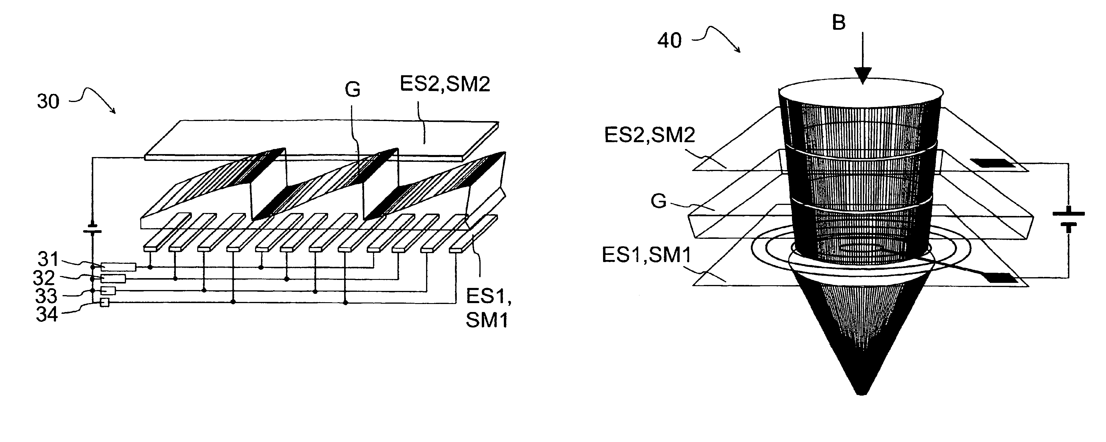
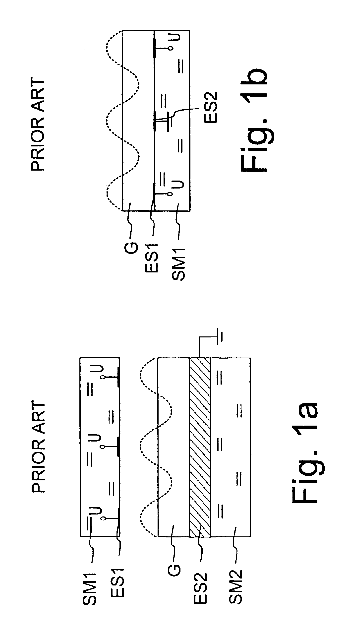
[0038]It is to be understood that the drawings presented hereinbelow are designed solely for purposes of illustration and thus, for example, not for showing the various components of the devices in their correct relative scale and / or shape. For the sake of clarity, the components and details which are not essential in order to explain the spirit of the invention have also been omitted in the drawings.

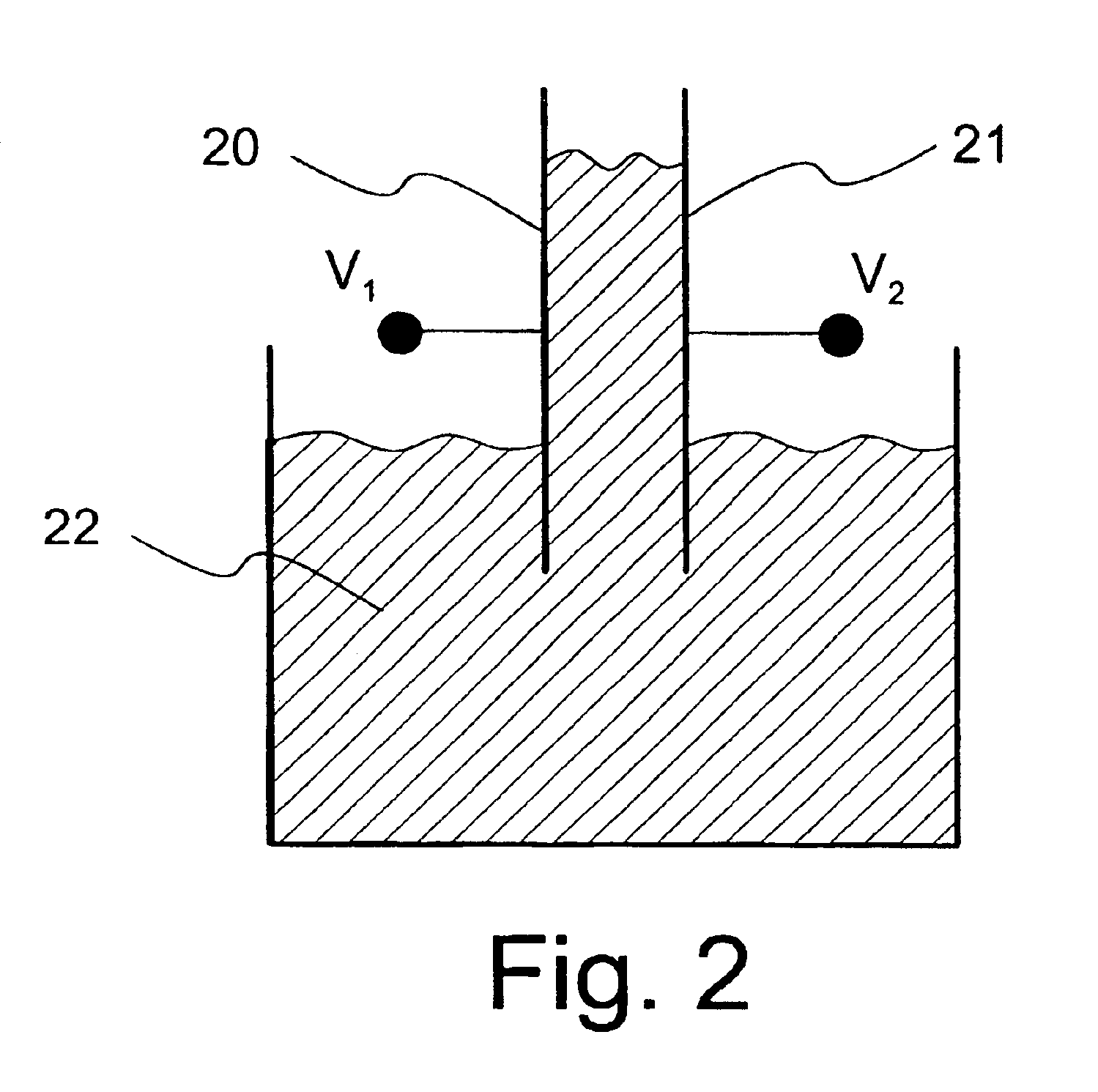
[0039]FIG. 2 illustrates the general principle of physics, which can be observed with dielectric substances. A dielectric substance can be defined as a substance in which an electric field may be maintained with zero or near zero power dissipation, i.e. the electrical conductivity is zero or near zero. In an electric field, the surface of two dielectrics with different dielectric constants is known to experience a force which is proportional to the square of the electric field strength. In FIG. 2 where an electric field is formed between electrode plates 20 and 21 of a field capacitor b...


PUM


Abstract

The invention refers to electrically reconfigurable optical devices based on the use of a layer of dielectric and transparent viscoelastic material (G) opposing at least a first electrode structure (ES1). According to the invention the arrangement of the individual electrode zones in the first electrode structure (ES1) in order to deform the viscoelastic layer (G) complies with one of the following alternatives. According to the first alternative, the electrode zones of the first electrode structure (ES1) are grouped into groups composed of two or more adjacent electrode zones and within each of said groups individual electrode zones are supplied each with a substantially different voltage. According to the second alternative, the electrode zones of the first electrode structure (ES1) are substantially annular, elliptical, rectangular or polygonal closed-loop electrodes. The invention allows, for example, for creating electrically reconfigurable blazed gratings (30) or Fresnel zone lenses (40).

Description

CROSS REFERENCE TO RELATED APPLICATIONS[0001]This application is for entry into the U.S. national phase under §371 for International Application No. PCT / FI02 / 00306 having an international filing date of Apr. 12, 2002, and from which priority is claimed under all applicable sections of Title 35 of the United States Code including, but not limited to, Sections 120, 363 and 365(c), and which in turn claims priority under 35 USC §119 to Finnish Patent Application No. 20010917 filed on May 3, 2001.TECHNICAL FIELD[0002]The present invention relates to electrically reconfigurable optical devices for diffracting an incident light wave. The invention also relates to a method for forming electrically reconfigurable optical devices for diffracting an incident light wave.BACKGROUND OF THE INVENTION[0003]Optical signals in different forms are today increasingly utilized in many different types of devices and applications. In order to take full advantage of systems including optical signals or be...

Claims


Application Information

Patent Timeline
IPC IPC(8): G02B26/08G02B5/18
CPCG02B5/1828G02B26/0833G02B26/0825G02B26/0808
Inventor SCHRADER, MARTIN
Owner INTELLECTUAL VENTURES I LLC
Why Eureka
Try Eureka