
Display device and method of manufacturing the same

a display device and active matrix technology, applied in the direction of organic semiconductor devices, electroluminescent light sources, thermoelectric devices, etc., can solve the problems of reducing display quality, reducing display uniformity, and difficulty in obtaining a sufficient opening ratio, so as to reduce display non-uniformity and enhance display quality.

Inactive Publication Date: 2005-05-31
JAPAN DISPLAY CENT INC
View PDF5 Cites 141 Cited by
  • Summary
  • Abstract
  • Description
  • Claims
  • Application Information

AI Technical Summary

Benefits of technology

[0008]The present invention has been made in consideration of the above problems, and an object of the invention is to provide a display device capable of suppressing display non-uniformity in a display screen and enhancing the display quality, and a method of manufacturing the same.
[0009]Another object of the invention is to provide a display device capable of increasing the degree of freedom in determining the screen size.
[0011]Still another object of the invention is to provide a method of manufacturing a display device without a decrease in productivity.

Problems solved by technology

It is thus difficult to obtain a sufficient opening ratio, posing a problem of how the efficiency in use of light is to be enhanced.
The use of transparent conductive material may lead to non-uniformity in electrode voltage in the screen plane of the light-emission-side electrode, degrading the display quality.
This problem becomes more conspicuous as the screen size increases.
Incidentally, another problem may arise that the screen size needs to be limited.
As has been stated above, in the prior art, it is difficult to use the active matrix display device using the top-face luminescence method.

Method used


Image

  • Display device and method of manufacturing the same
  • Display device and method of manufacturing the same
  • Display device and method of manufacturing the same

Examples


Embodiment Construction

[0039]An active matrix type planar display device according to an embodiment of the present invention will now be described in detail with reference to the accompanying drawings. In this embodiment, a self-luminescence type display device, more specifically, an organic EL display device, is described as the active matrix type planar display device.

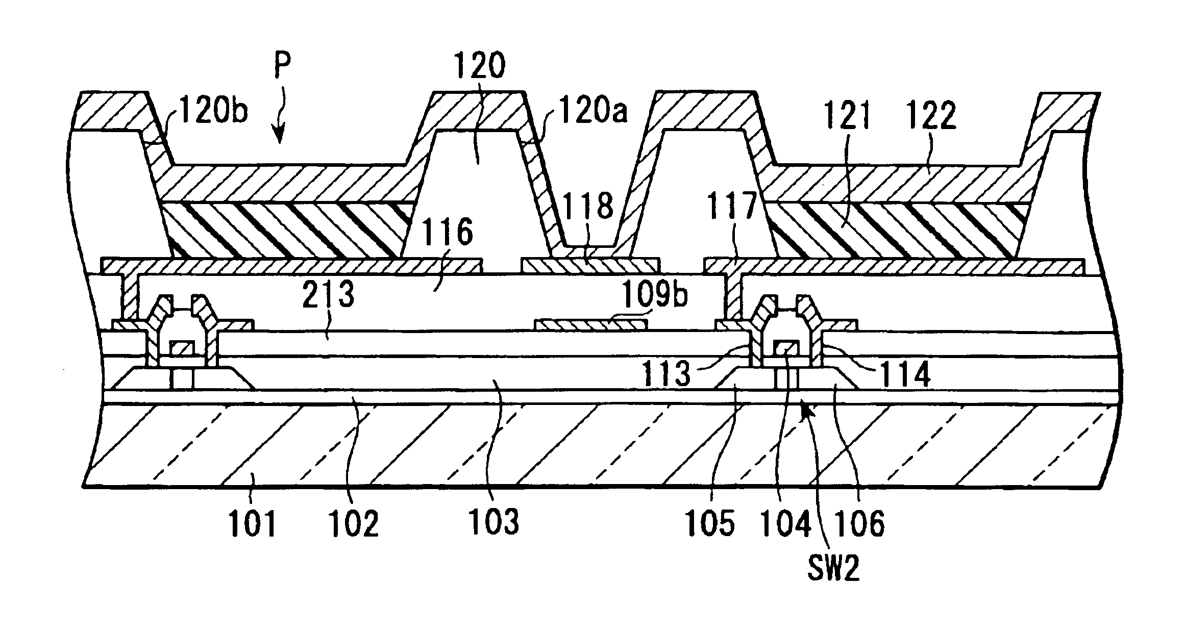
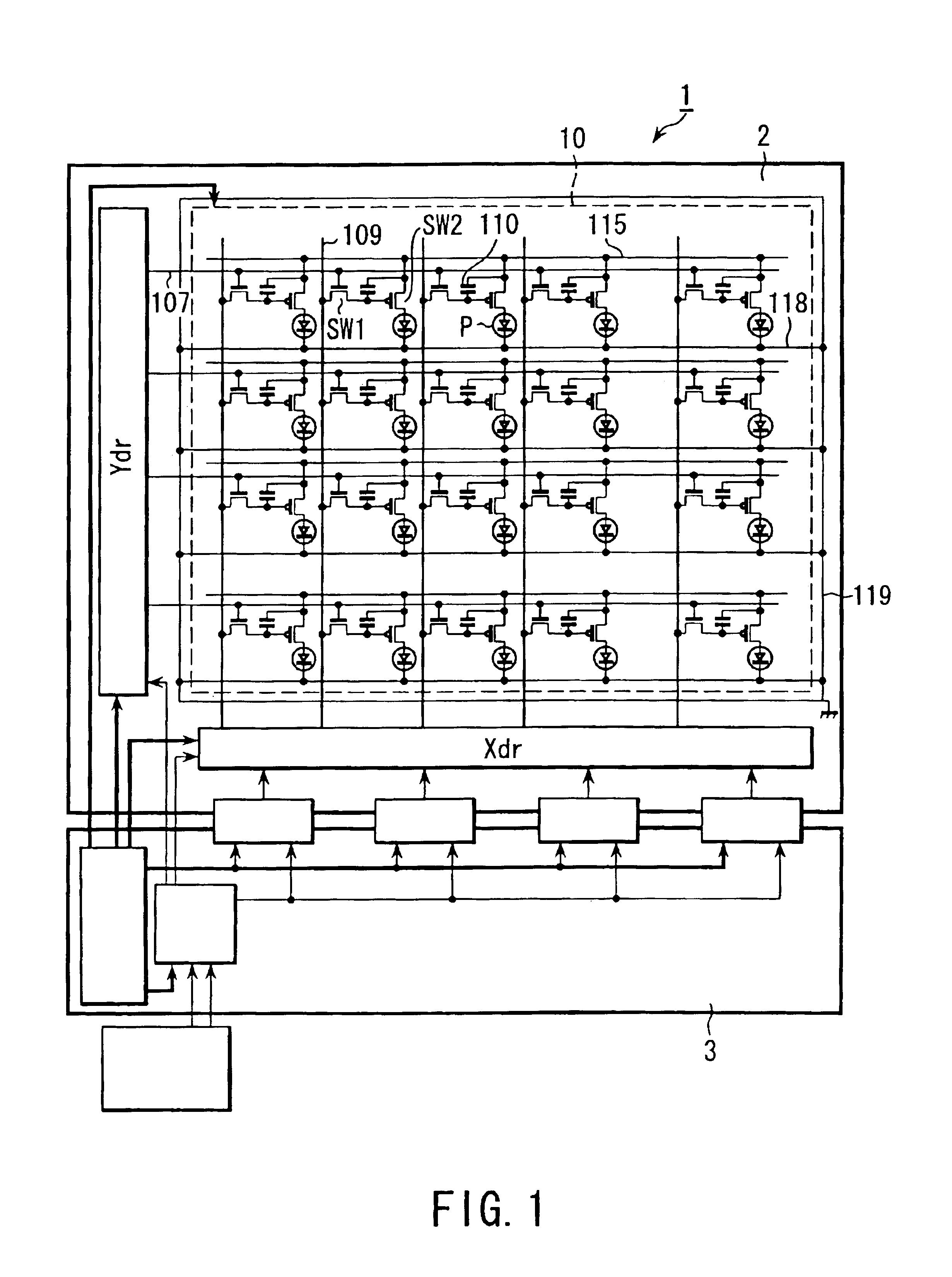
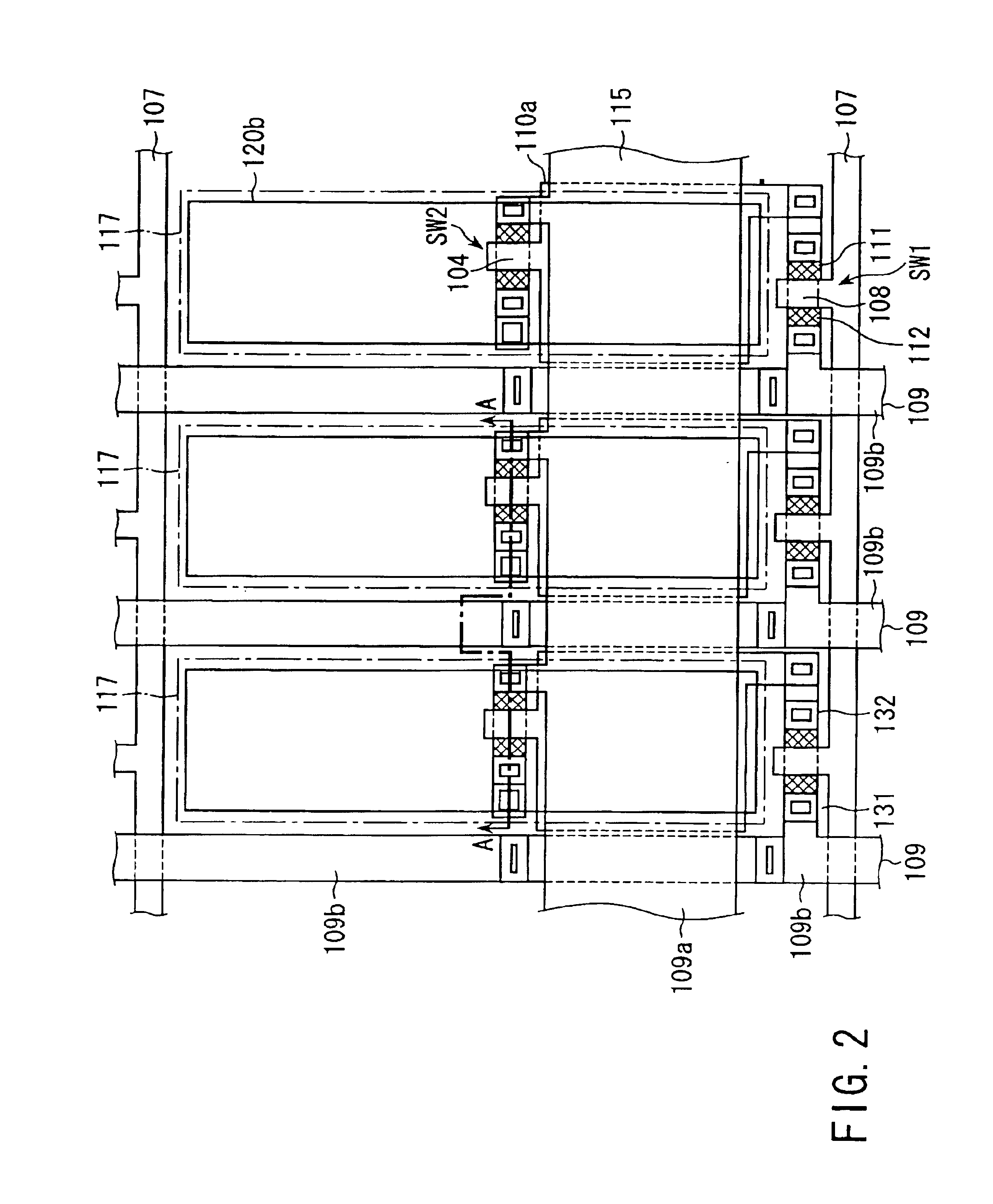
[0040]FIG. 1 is a plan view schematically showing the structure of an organic EL display device according to an embodiment of the present invention. FIG. 2 is a partial plan view schematically showing the structure of a display region of the organic EL display device shown in FIG. 1. FIG. 3 is a cross-sectional view taken along line A—A in FIG. 2.

[0041]As is shown in FIGS. 1-3, an active matrix type organic EL display device 1 comprises an organic EL panel 2 and an external drive circuit 3 for driving the organic EL panel 2. The organic EL panel 2 comprises three kinds of display elements P, which respectively emit red, green and blue ligh...


PUM


Abstract

An active matrix type planar display device includes display elements arranged in a matrix and auxiliary wiring elements. The display element has an optical active layer between a first electrode formed on a substrate and a second electrode. The auxiliary wiring element is formed in the same layer or on the same surface as the first electrode, electrically insulated from the first electrode, and electrically connected to the second electrode.

Description

BACKGROUND OF THE INVENTION[0001]The present invention relates to a planar display device such as an organic electroluminescence (EL) display device, and a method of manufacturing the same. In particular, this invention relates to an active matrix type planar display device and a method of manufacturing the same.[0002]There has been an increasing demand for planar display devices, represented by liquid crystal displays, which are thinner, lighter and less in power consumption than CRT display devices. In particular, active matrix type planar display devices, wherein each display element is provided with a switching device, have been applied to various displays of mobile information apparatuses, etc. The active matrix planar display device has a high display quality, with no crosstalk between adjacent display elements.[0003]Recently, organic electroluminescence (EL) display devices have been widely developed as self-luminescence type displays, which realize higher response speeds and...

Claims


Application Information

Patent Timeline
IPC IPC(8): H01L27/32H01L27/28H05B33/26H01L51/52
CPCH01L27/3244H01L51/5228H01L51/5218H01L27/3246H01L27/3276H01L2251/5315H01L51/5234H01L51/5284H10K59/122H10K59/1315H10K59/131H10K2102/3026H10K59/80518H10K59/80522H10K59/80524H05B33/26H10K59/12H10K50/818H10K50/824H10K50/828H10K50/865
Inventor KOBAYASHI, MICHIYAYAMAMOTO, KAZUSHIGE
Owner JAPAN DISPLAY CENT INC
Learn More