Data processing method and apparatus, reticle mask, exposing method and apparatus, and recording medium
- Summary
- Abstract
- Description
- Claims
- Application Information
AI Technical Summary
Benefits of technology
Problems solved by technology
Method used
Image
Examples
first embodiment
[0053
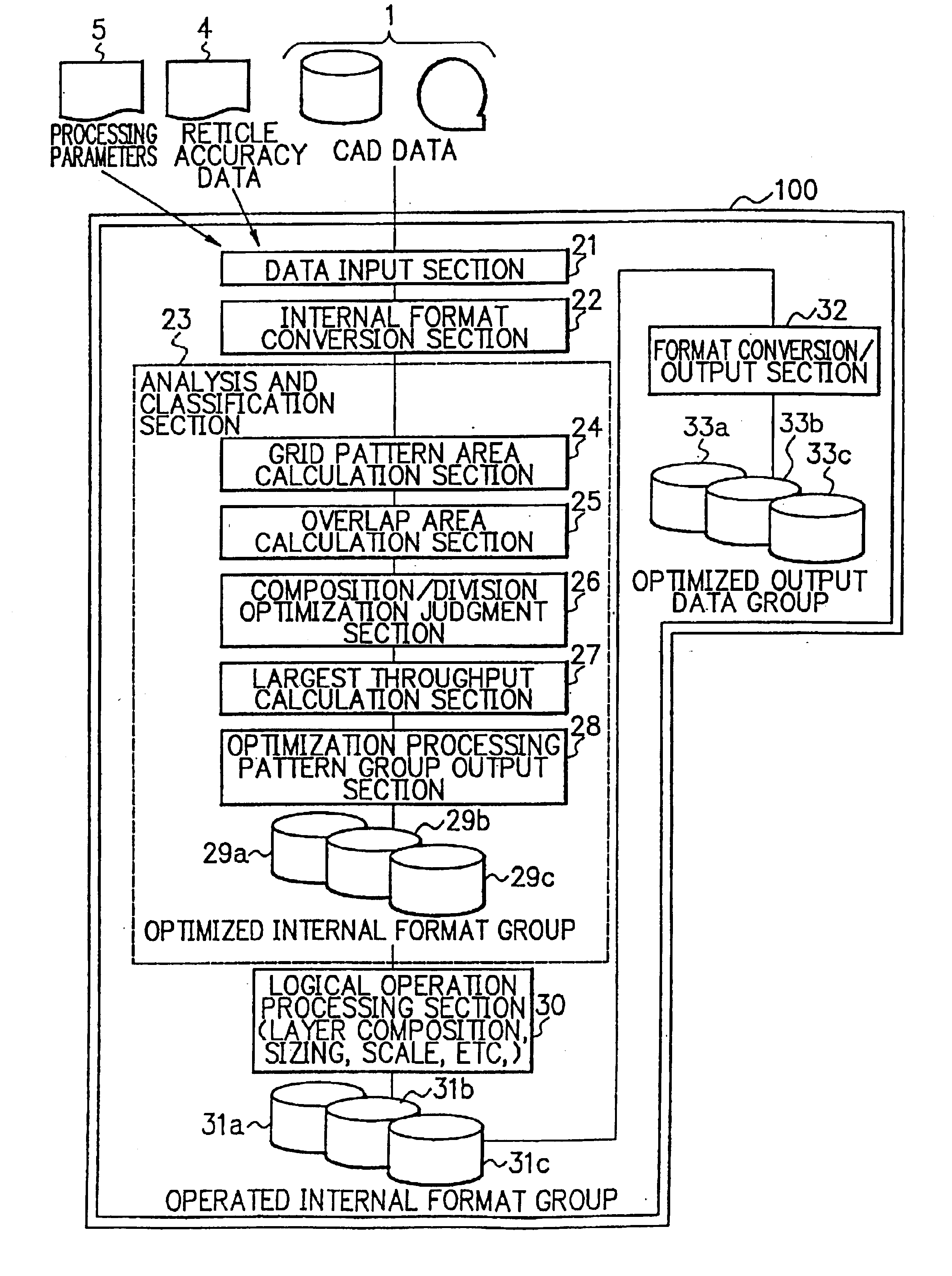
[0054]FIG. 5 is a block diagram showing the construction of a data processing apparatus according to the first embodiment of the present invention. FIGS. 6A to 6G are charts for illustrating operations of the analysis and classification section shown in FIG. 5. The first embodiment of the present invention will be described below with reference to these FIGS. 5 and 6A to 6G.
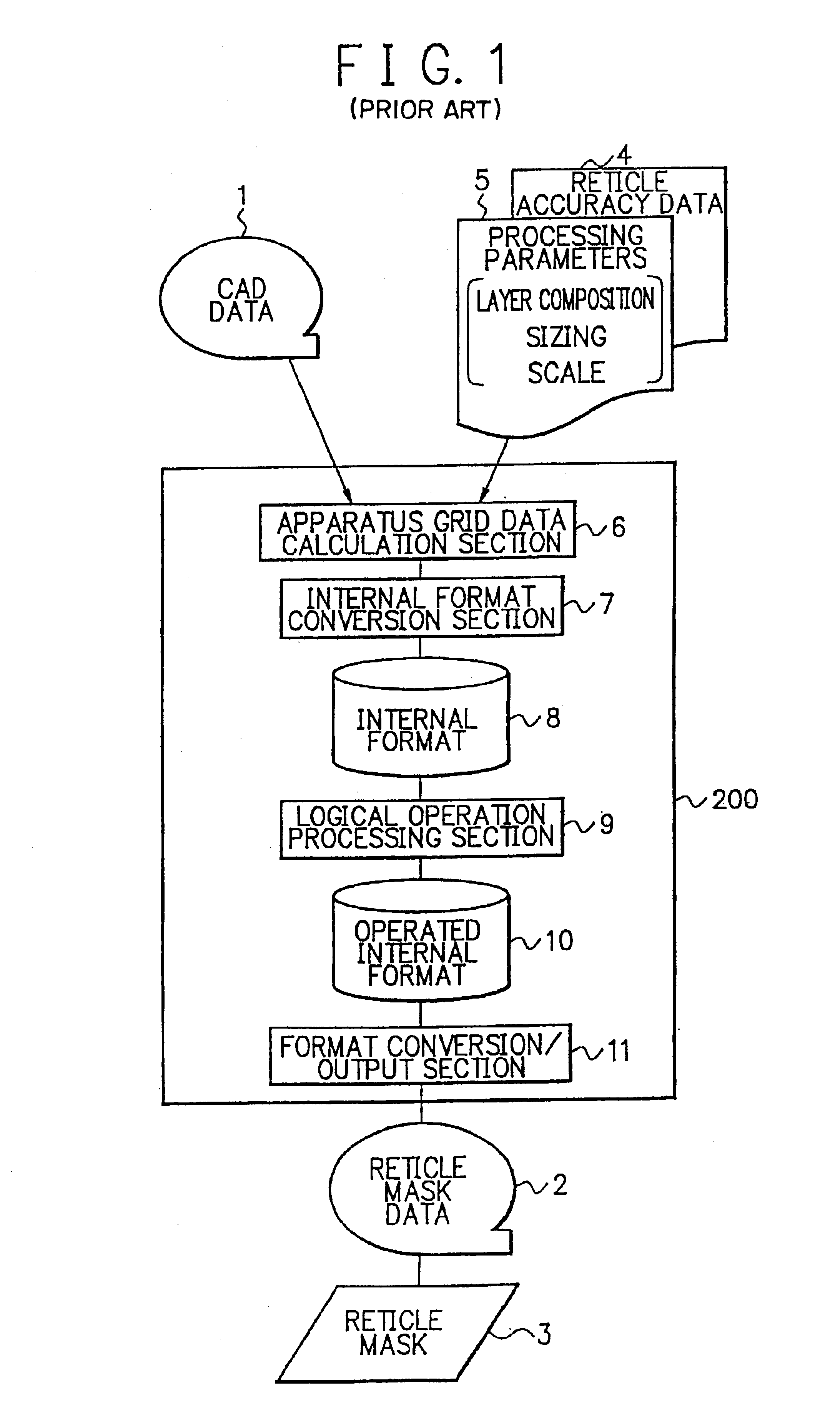
[0055]Referring to FIG. 5, CAD data 1 is design data that symbolically represents circuit layouts of, e.g., a semiconductor device being manufactured. Reticle accuracy data 4 gives information on permissible range of error in printing on wafers with a reticle mask made on the basis of the CAD data 1. Processing parameters 5 include various data such as layer composition data, sizing data, and scale data, as described before.
[0056]The data processing apparatus 100 according to this embodiment makes reticle mask data representing an layout pattern used as an original for processing wafers, on the basis of the ...
second embodiment
[0097
[0098]Next, the second embodiment of the present invention will be described. FIG. 9 is a block diagram showing the construction of a data processing apparatus according to the second embodiment. In FIG. 9, each block representing the same function as that in FIG. 5 is denoted by the same reference as that in FIG. 5. In the above first embodiment, logical operation such as layer composition, sizing, or enlargement, is performed after optimization of grid data for each layer. Contrastingly in the second embodiment, such logical operation is performed before optimization of grid data.
[0099]As shown in FIG. 9, a logical operation processing section 61 performs logical operation to CAD data 1, reticle accuracy data 4, and processing parameters 5 being input through the data input section 21. Operated internal format data 62 is thereby made. The analysis and classification section 23 performs data processing to the internal format data 62 in the same manner as that described with FI...
third embodiment
[0105
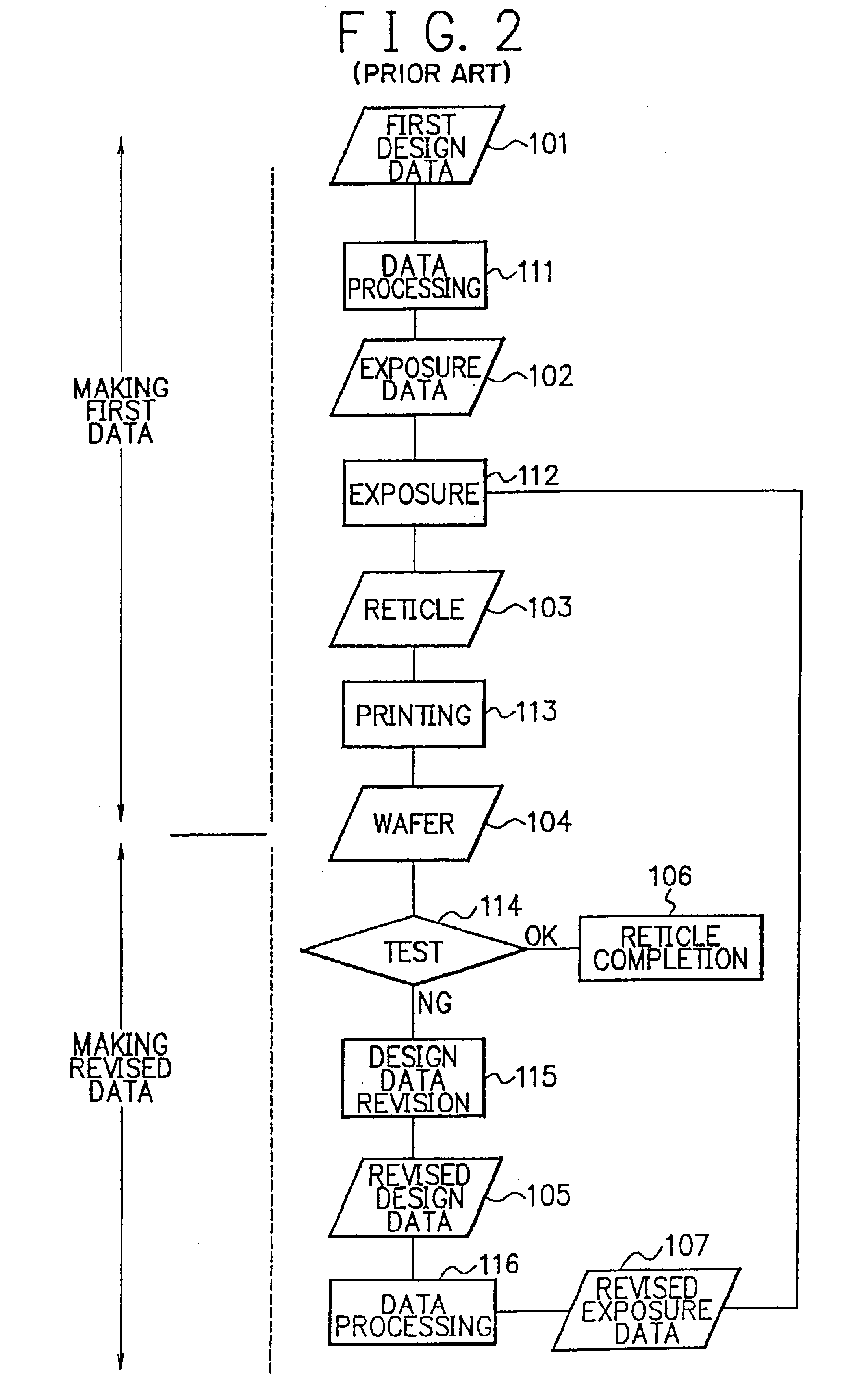
[0106]Next, the third embodiment of the present invention will be described. FIG. 10 is a block diagram showing the construction of each of a data processing apparatus and an exposing apparatus according to the third embodiment. In FIG. 10, design data 71 made by CAD, symbolically represents circuit layouts of a semiconductor device being manufactured. The design data 71 includes first design data 101 and revised design data 105 as shown in FIG. 2.
[0107]The data processing apparatus 300 according to this embodiment comprises a design data input section 72, a revise position designation section 73, and a data processing section 74, to make exposure data representing a reticle pattern used as an original for processing wafers, from the design data 71. The design data input section 72 is for inputting the first or revised design data 71 into the data processing apparatus 300. The design data input section 72 comprises, e.g., an input device such as a keyboard or a mouse of a compu...
PUM
 Abstract
Description
Claims
Application Information
 - R&D
- Intellectual Property
- Life Sciences
- Materials
- Tech Scout
- Unparalleled Data Quality
- Higher Quality Content
- 60% Fewer Hallucinations
Browse by: Latest US Patents, China's latest patents, Technical Efficacy Thesaurus, Application Domain, Technology Topic, Popular Technical Reports.
© 2025 PatSnap. All rights reserved.Legal|Privacy policy|Modern Slavery Act Transparency Statement|Sitemap|About US| Contact US: help@patsnap.com


