Image sensor having uniform sensitivity
a technology of image sensor and sensitivity, which is applied in the field of image sensor, can solve the problems of undulation due to interference, uniform spectral sensitivity characteristic of the line sensor ics b>7/b>, etc., and achieve the effects of uniform output levels of red, small dispersion of electromotive force of the sensor element, and high sensitivity
- Summary
- Abstract
- Description
- Claims
- Application Information
AI Technical Summary
Benefits of technology
Problems solved by technology
Method used
Image

Examples
first embodiment
A first embodiment of the present invention will be described below with reference to FIGS. 1A, 1B and 2.
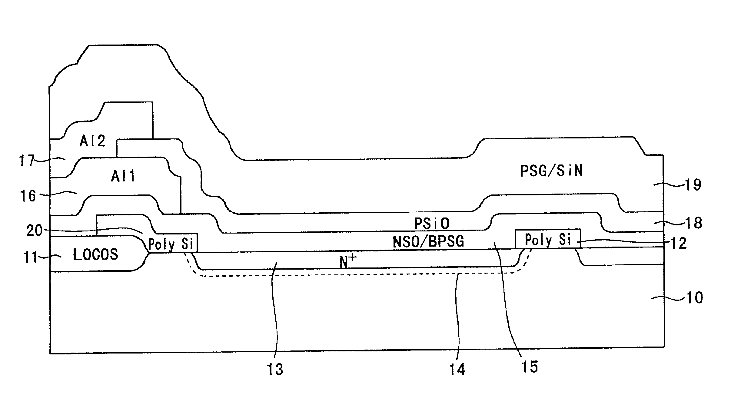
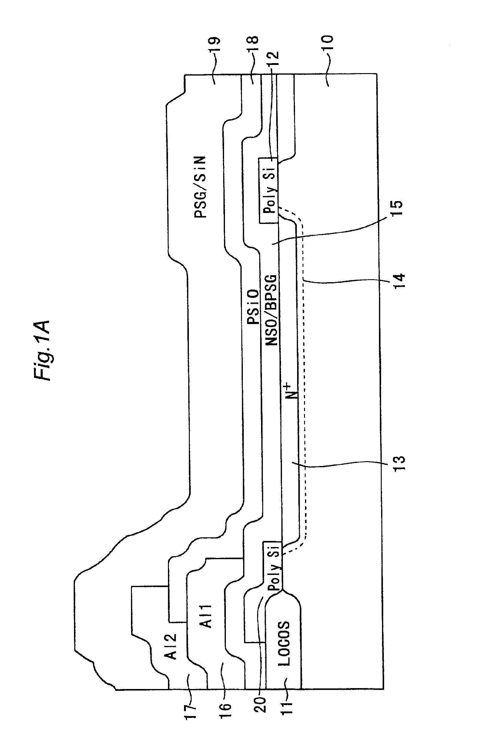
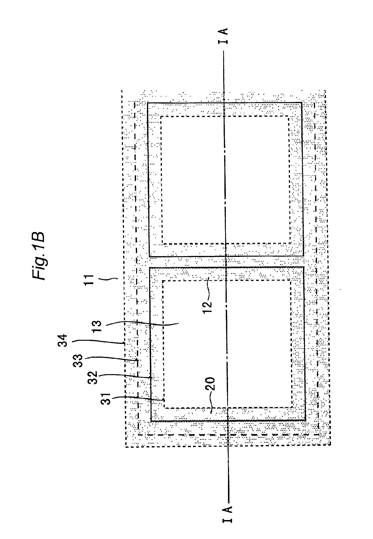
FIG. 1A is a sectional view showing a structure of a line sensor IC according to a first embodiment of the present invention. In FIG. 1A, reference numeral 10 denotes a p-type semiconductor substrate; 11, a LOCOS layer formed locally on the semiconductor substrate 10; 12, a polysilicon layer formed on the semiconductor substrate 10 so as to be separated from the LOCOS layer 11; 20, another polysilicon layer provided on the top surface of the LOCOS layer 11 to cover part of the LOCOS layer 11 and having one end portion (right end portion in FIG. 1A) that extends toward the polysilicon layer 12; 13, a n+ sensor portion formed by implanting a n-type impurity into a portion of the substrate 10 that is located between the polysilicon layer 12 and another polysilicon layer 20; and 14, a depletion layer formed along the n+ sensor portion 13. The depletion layer 14 includes space charge ...
second embodiment
Next, a second embodiment of the present invention will be described.
In this embodiment, the thickness of the protective film 19 is set at 2,000 Å or less.
Where the thickness of the protective film 19 is reduced in this manner, undulations in the transmission spectrum due to interference of incident light are made small and the degrees of light absorption at the respective wavelengths of red, green, and blue are decreased. As a result, color-related variations among sensor outputs are reduced.
FIG. 3 shows a transmission spectrum of the protective film 19 having such a thickness.
As in the case of FIG. 8, the horizontal axis represents the wavelength and the vertical axis represents the transmittance.
As seen from FIG. 3, transmittance values at wavelengths 460 nm, 530 nm, and 640 nm are about 85%, about 75%, and about 90%, respectively. Undulations in the spectrum are small in this embodiment. This is in contrast to the spectrum of FIG. 8 of the conventional protective film having the...
third embodiment
Next, a third embodiment of the invention will be described.
In the second embodiment, sensor output variation among colors is reduced by decreasing the thickness of the protective film 19 to 2,000 Å or less. In this third embodiment, instead of decreasing the thickness of the protective film 19, the protective film 19 is so formed as to have superior UV transmission characteristic. Namely, the concentration of Si—H bonds is made relatively lower than that of N—H bonds in the protective film 19, to make the degree of absorption in a short wavelength range lower than in the conventional protective film 19,.
With this measure, the degree of light absorption in the short wavelength range is lowered and hence the transmittance is increased in a wavelength range around 460 nm. As a result, variations among outputs of the three respective colors are reduced and the same advantages as in the second embodiment are obtained.
PUM
 Abstract
Description
Claims
Application Information
 - R&D
- Intellectual Property
- Life Sciences
- Materials
- Tech Scout
- Unparalleled Data Quality
- Higher Quality Content
- 60% Fewer Hallucinations
Browse by: Latest US Patents, China's latest patents, Technical Efficacy Thesaurus, Application Domain, Technology Topic, Popular Technical Reports.
© 2025 PatSnap. All rights reserved.Legal|Privacy policy|Modern Slavery Act Transparency Statement|Sitemap|About US| Contact US: help@patsnap.com