
Apparatus and method for removably adhering a semiconductor substrate to a substrate support

a technology of adhesives and semiconductor substrates, applied in the direction of weaving, manufacturing tools, transportation and packaging, etc., can solve the problems of high voltage requirements, damage to the substrate, and usually required additional hardwar

Inactive Publication Date: 2004-04-20
KLA TENCOR TECH CORP
View PDF2 Cites 38 Cited by
  • Summary
  • Abstract
  • Description
  • Claims
  • Application Information

AI Technical Summary

Problems solved by technology

However, the primary disadvantage of edge gripping or clamping mechanisms is that they may cause damage to the substrate during the exercise of mechanical force on the substrate.
Furthermore, additional hardware is usually required to insert and extract the substrate to and from the clamping mechanism.
While the problems of mechanical damage to the substrate and positioning the substrate to lie flat on the substrate support are not encountered as often when using an electrostatic chucking mechanism, there are many disadvantages distinctive to electrostatic chucks as well, including high voltage requirements, dangerous stored energy, the need for complex mechanical and electrical apparatus, premature release of the substrate in vacuum, dependance on the substrate for chucking effectiveness, expense of the equipment, large size (both in weight (heavy) and dimensions.

Method used


Image

  • Apparatus and method for removably adhering a semiconductor substrate to a substrate support
  • Apparatus and method for removably adhering a semiconductor substrate to a substrate support
  • Apparatus and method for removably adhering a semiconductor substrate to a substrate support

Examples


Embodiment Construction

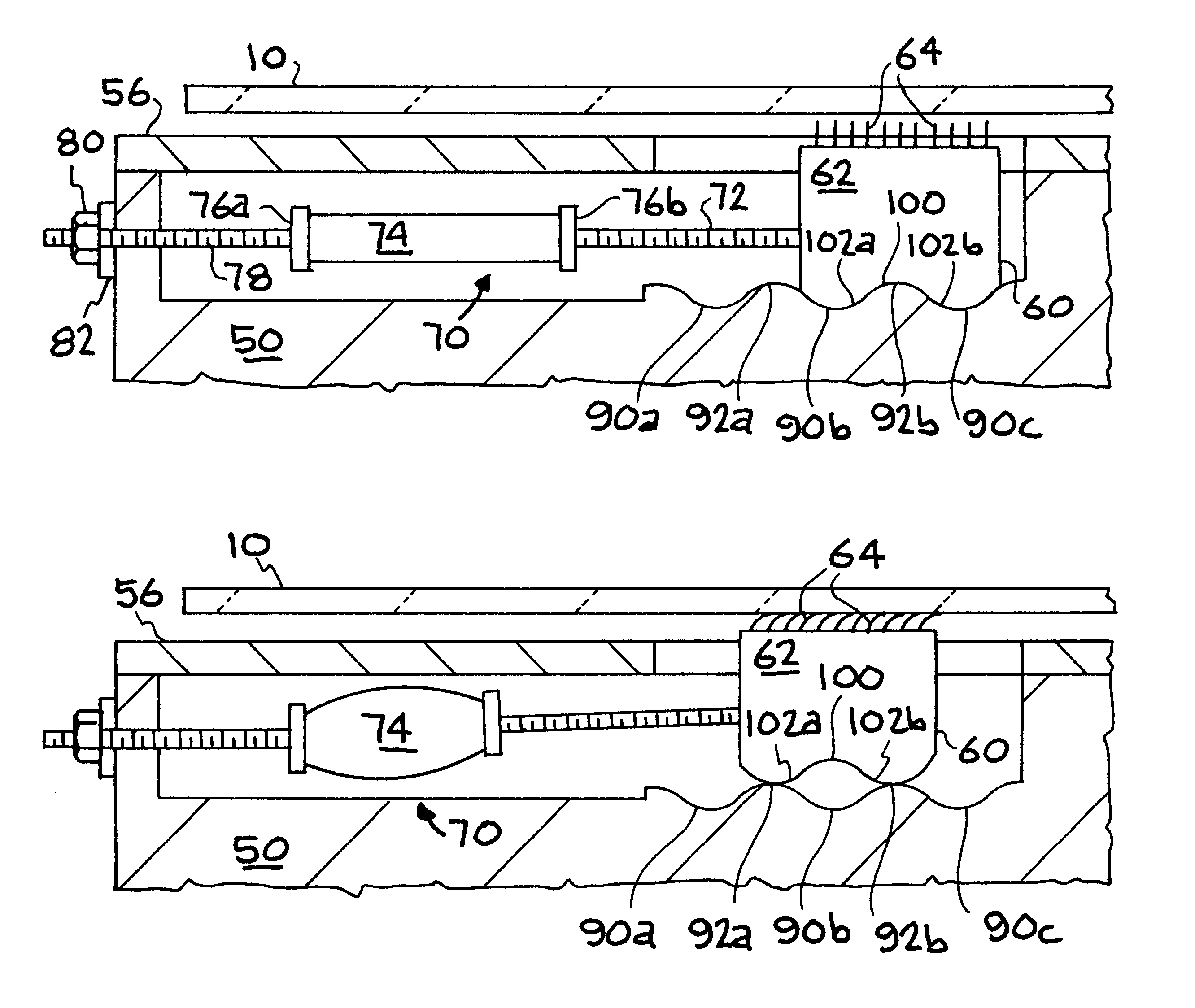
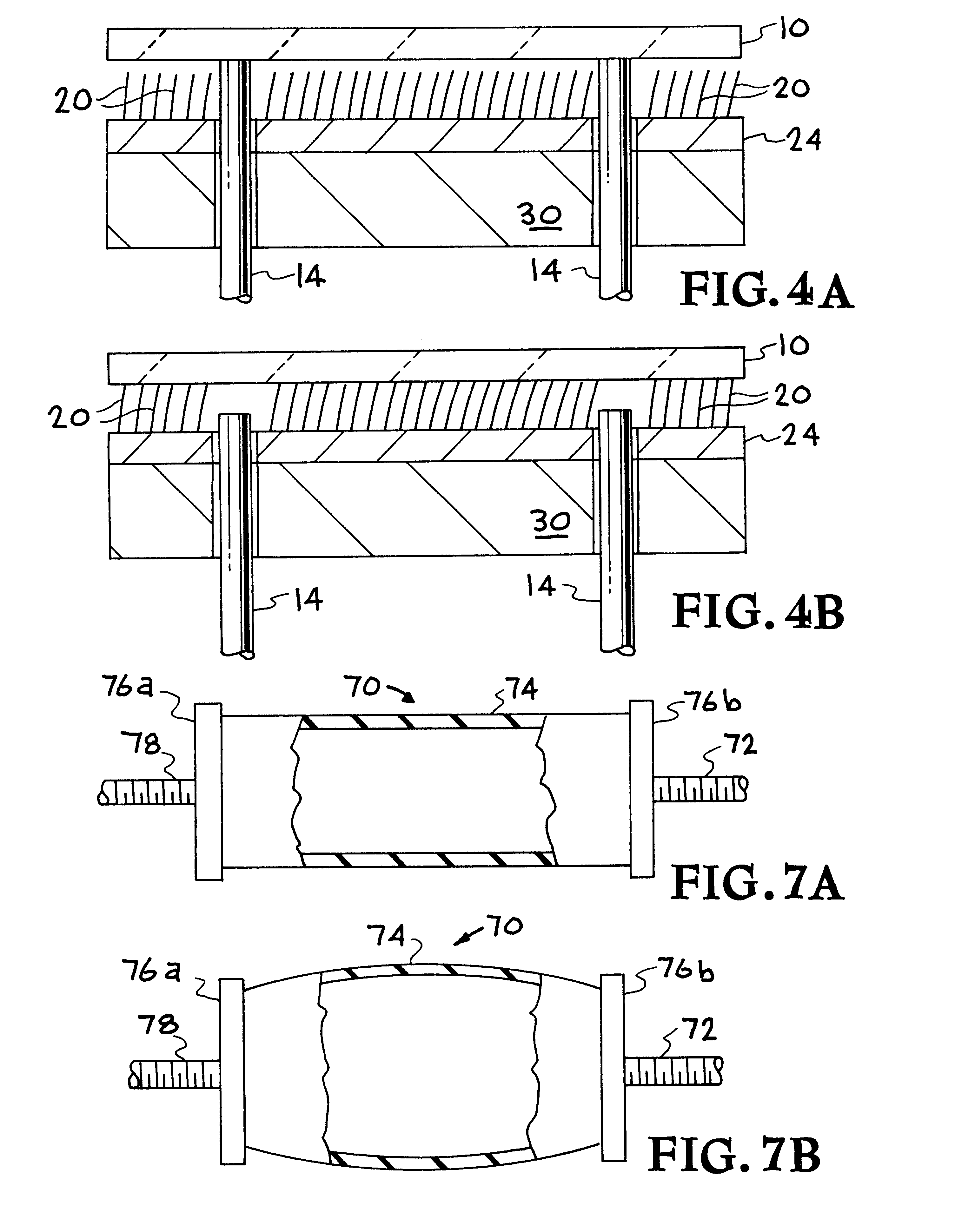
Turning to FIGS. 4A and 4B, the invention, in its simplest form, is illustrated wherein a substrate 10 is shown, in FIG. 4A, resting on withdrawable ejection pins 14 over a substrate support 30 within a processing chamber such as a vacuum chamber (not shown). A plurality of fibers 20 below substrate 10 (and shown in both enlarged length and diameter for illustrative purposes only) are secured to a mounting plate 24 which, in turn, is mounted on substrate support 30. Fibers 20 are shown, in FIG. 4A, just barely touching or out of touch with the under surface of substrate 10.

When pins 14 are retracted, as shown in FIG. 4B, substrate 10 comes into contact with and rests on all of the tops of fibers 20 which then act to secure substrate 10 to substrate support 30 through the contact between substrate 10 and fibers 20 and the securement of mounting plate 24 to substrate support 30. Substrate 10 is then processed in the vacuum chamber while substrate 10 remains secured to substrate suppor...


PUM

PropertyMeasurementUnit
Forceaaaaaaaaaa
Pressureaaaaaaaaaa
Structureaaaaaaaaaa

Abstract

A process and apparatus is disclosed capable of removably adhering a semiconductor substrate to a substrate support in a sub-atmospheric environment using a plurality of individual fibers, each mounted at one end adjacent the substrate support, and each having a loose end. When the portions of the fiber adjacent the loose fiber ends are each brought into contact with the under surface of the substrate, Van der Waals forces are exerted between the substrate and the fibers to urge the substrate toward the underlying substrate support. In a preferred embodiment, the substrate and portions of the fiber adjacent the loose fiber ends are first vertically brought into physical contact with one another, and then a horizontal force is applied to horizontally move, with respect to one another, the substrate and the portions of the fibers adjacent the loose fiber ends. After application of the horizontal force, a vertical force is applied between the substrate and the fibers of sufficient strength to urge the substrate and the fibers away from one another without breaking contact between the substrate and the portions of the fiber adjacent the fiber ends to thereby place tension on the substrate to urge the substrate to lie flat against the underlying substrate support.

Description

1. Field of the InventionThis invention relates to integrated circuit structures. More particularly, this invention relates to a chucking structure useful for securing a semiconductor substrate to a substrate support during the formation and / or testing of an integrated circuit structure thereon, particularly in a vacuum environment.2. Description of the Related ArtIn the construction of integrated circuit structures on semiconductor substrates, the substrate is normally secured to an underlying substrate support in a vacuum environment by one of two conventional means, an edge gripping mechanical clamping structure, or an electrostatic chuck.While edge gripping mechanical clamping structures keep the substrate from slipping, i.e. keep the substrate from horizontally sliding or moving on the substrate support, such an edge gripping mechanical clamping structure does not flatten the substrate to the underlying substrate support. Since some substrates, such as single crystal silicon se...

Claims


Application Information

Patent Timeline
IPC IPC(8): H01L21/00
CPCH01L21/67092Y10S29/90Y10T29/49126Y10T29/49133Y10T279/23Y10T29/53265Y10T428/23914
Inventor LENT, MATTHEW HARRIS
Owner KLA TENCOR TECH CORP
Learn More