Tunneling transistor applicable to nonvolatile memory
a transistor and non-volatile memory technology, applied in the direction of diodes, semiconductor devices, electrical apparatus, etc., can solve the problems of inapplicability to the miniaturization of semiconductor integrated circuits having memory circuits, inability to control the current passing through the channel by the gate voltage,
- Summary
- Abstract
- Description
- Claims
- Application Information
AI Technical Summary
Problems solved by technology
Method used
Image
Examples
first embodiment
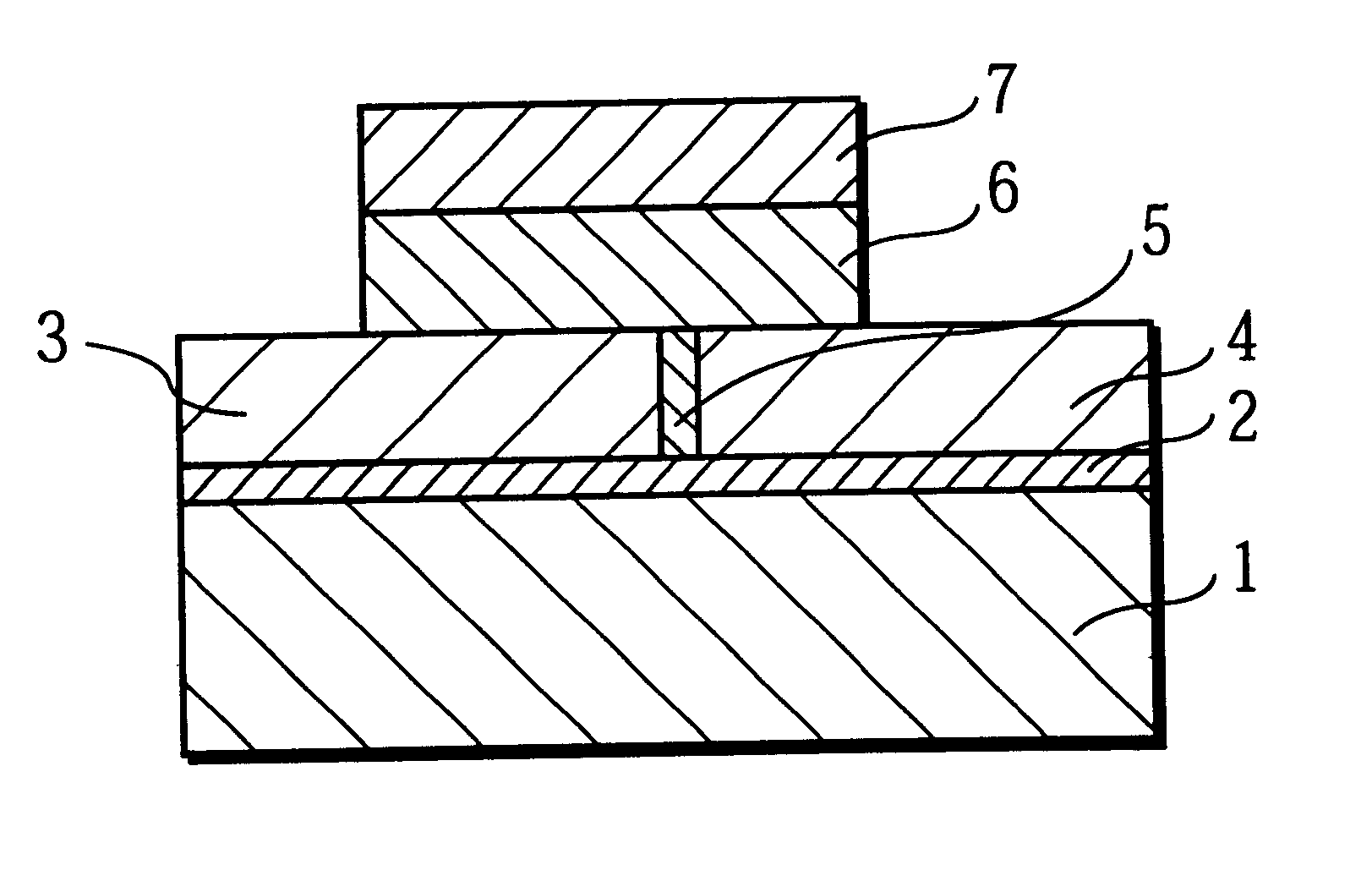
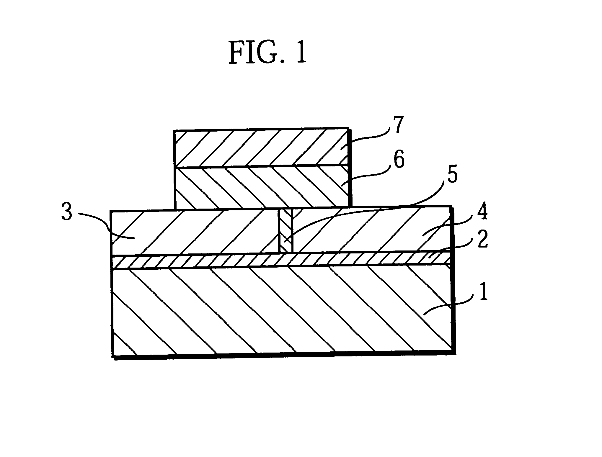
FIG. 1 is a schematic sectional view showing the construction of a tunneling transistor according to the first embodiment of the invention. In the figure, a first insulating layer 2 made of a silicon oxide (SiO.sub.2) or the like is formed on a silicon substrate 1. A source 3 made of n-type silicon and a drain 4 made of n-type silicon are formed on the first insulating layer 2, with an insulator 5 that provides a tunnel barrier being interposed between the source 3 and the drain 4. This insulator 5 is made of a silicon oxide (SiO.sub.2) or the like. A ferroelectric layer 6 is formed on top of the source 3, insulator 5, and drain 4. A gate electrode 7 is disposed on the ferroelectric layer 6.
In this embodiment, the ferroelectric layer 6 is positioned immediately above the source 3 and the drain 4. To prevent n-type silicon which constitutes the source 3 and the drain 4 from being oxidized and thereby becoming an insulator, a ferroelectric material of low oxidizing power such as BaF.s...
second embodiment
FIG. 5 is a schematic sectional view showing the construction of a tunneling transistor according to the second embodiment of the invention. As shown in the figure, this tunneling transistor differs with the first embodiment in that a second insulating layer 8 and a floating electrode 9 are interposed between the source 3, the insulator 5, and the drain 4 on one side and the ferroelectric layer 6 on the other side. The following explanation focuses on the difference with the first embodiment.
The floating electrode 9 is provided to keep the ferroelectric layer 6 from direct contact with the source 3 and the drain 4. As mentioned earlier, when the ferroelectric layer 6 is made of an oxide, part of the surfaces of the source 3 and drain 4 that comes into contact with the ferroelectric layer 6 may be oxidized, thereby forming a thin insulator. Besides, the composition of the ferroelectric 6 changes during the growth of crystals, causing unstable growth of the ferroelectric crystals. Alt...
third embodiment
In the first and second embodiments, the tunneling transistor is constructed such that the insulator 5 of a few nanometers in thickness through which a tunneling current flows is formed between the source 3 and the drain 4. Such a construction, though applicable when fabricating a small number of semiconductor devices, may not be suitable for fabrication of a large number of identical semiconductor devices in an integrated circuit. Considering this, the third embodiment presents a construction that lends itself to fabrication of a substantial number of semiconductor devices on a single substrate.
FIG. 6 is a schematic sectional view showing the construction of a tunneling transistor according to the third embodiment of the invention. As illustrated, the drain 4 made of n-type silicon is formed on the silicon substrate 1, and the insulator 5 made of a silicon oxide (SiO.sub.2) is deposited on the silicon substrate 1 and the drain 4. The source 3 made of n-type silicon is formed on the...
PUM
 Abstract
Description
Claims
Application Information
 - R&D
- Intellectual Property
- Life Sciences
- Materials
- Tech Scout
- Unparalleled Data Quality
- Higher Quality Content
- 60% Fewer Hallucinations
Browse by: Latest US Patents, China's latest patents, Technical Efficacy Thesaurus, Application Domain, Technology Topic, Popular Technical Reports.
© 2025 PatSnap. All rights reserved.Legal|Privacy policy|Modern Slavery Act Transparency Statement|Sitemap|About US| Contact US: help@patsnap.com


