
Metal core multilayer resin wiring board with thin portion and method for manufacturing the same

a multi-layer resin and metal core technology, applied in the field of multi-layer resin wiring boards, can solve the problems of increased possibility of drill bit breakage, long time required, and significant difficulty in drilling

Inactive Publication Date: 2001-11-27
NGK SPARK PLUG CO LTD
View PDF7 Cites 159 Cited by
  • Summary
  • Abstract
  • Description
  • Claims
  • Application Information

AI Technical Summary

Benefits of technology

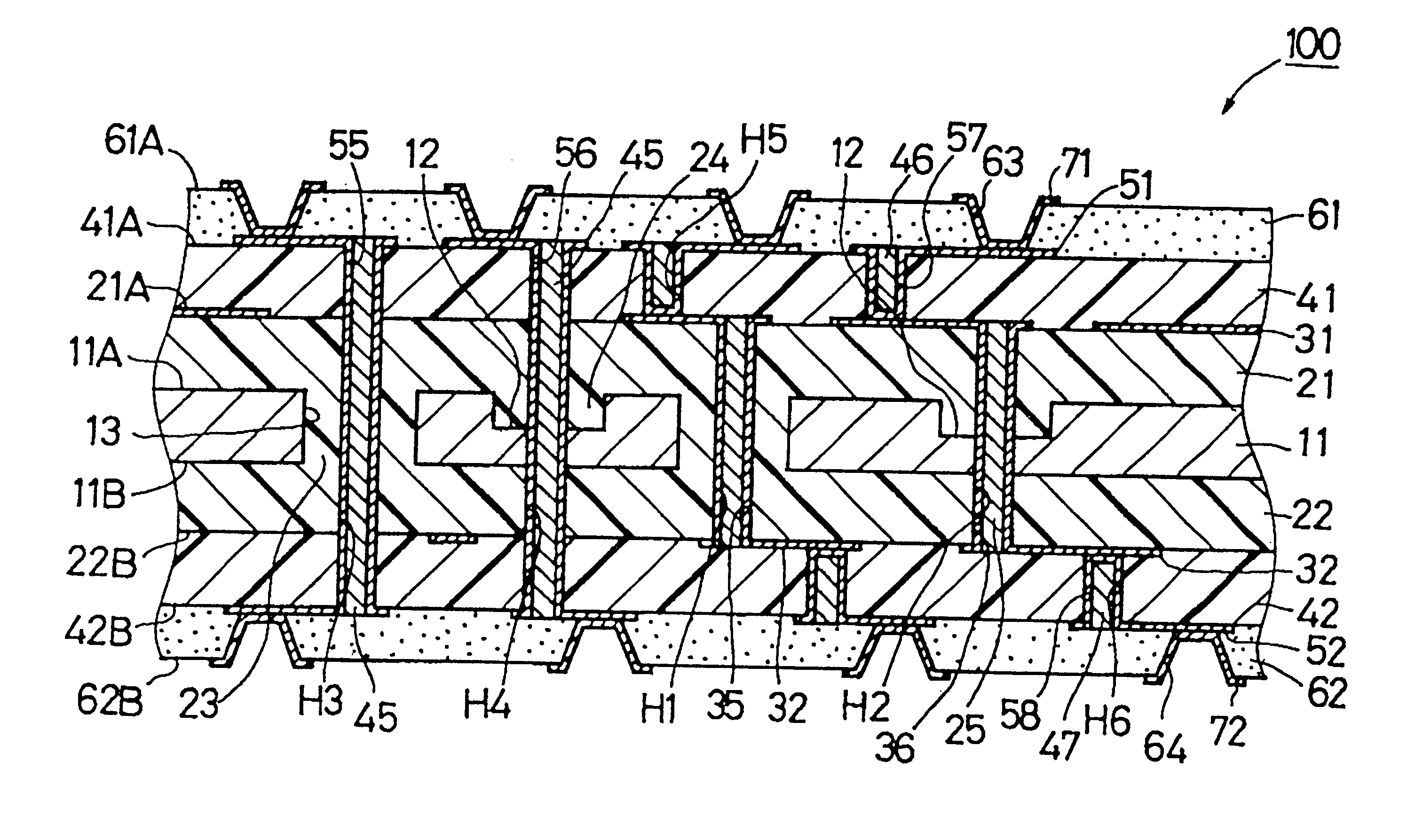
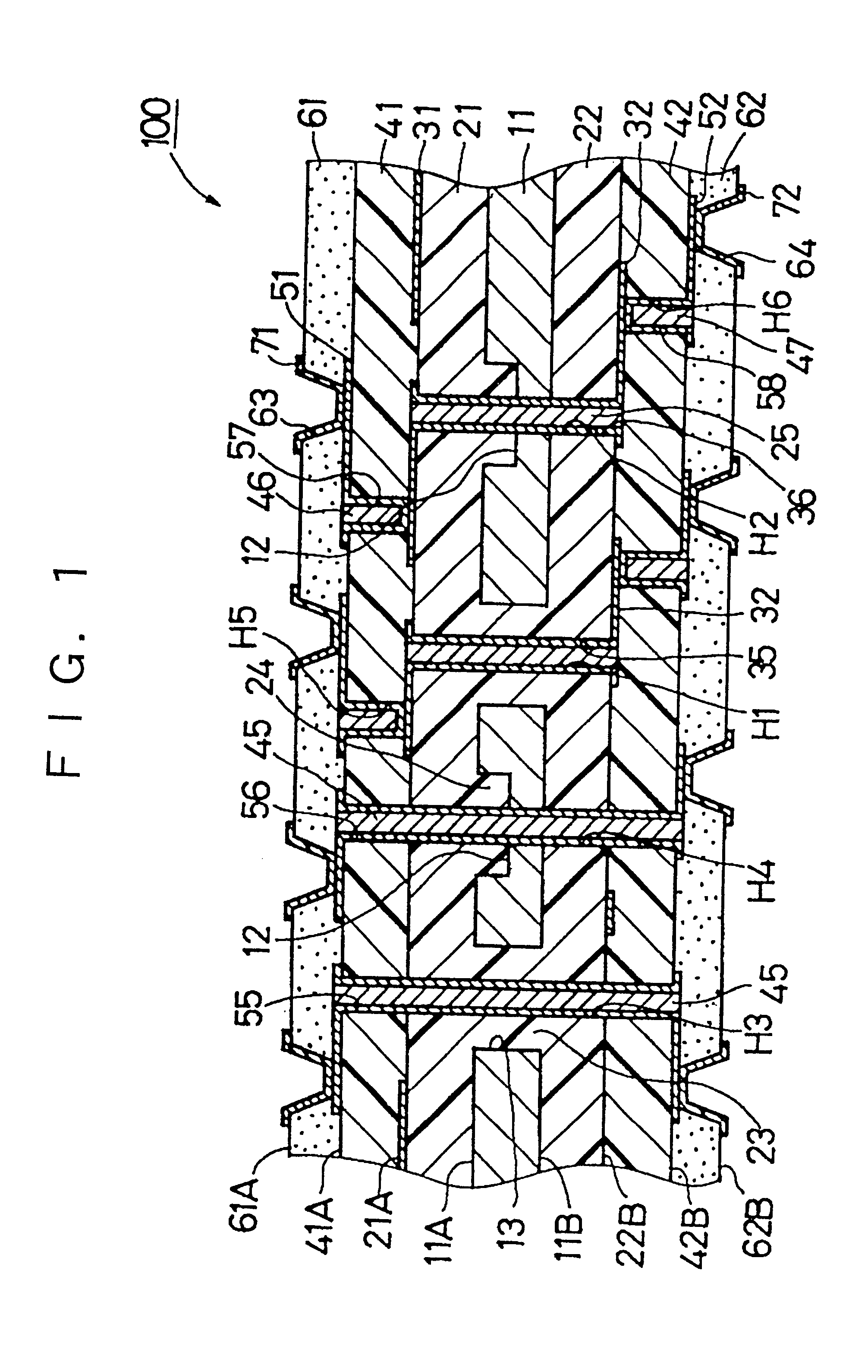
To increase the rigidity of the metal core substrate and thus facilitate the handling and yield, portions of the metal core substrate of the present PWB, other than the thin portion, can be rendered relatively thick. Since an increase in the rigidity of the metal core substrate leads to an increase in the rigidity of the multilayer resin wiring board, the board hardly warps, undulates, or deforms, thereby establishing reliable connection to electronic devices, such as IC chips, and other resin wiring boards, such as a mother board or a junction board. When the through hole for connection to the metal core substrate is formed by laser machining, fine thin holes can be formed a high speed and at a high degree of accuracy as in the case of formation of through holes in a thin metal core substrate. Further, deterioration of the insulating resin layer at a portion around the bored through hole can be suppressed. Accordingly, the multililayer resin wiring board obtained from the present invention has a low cost and high rigidity while further having highly accurate, fine vias connected to the metal core substrate.
In the method for manufacturing a multilayer resin wiring board according to the present invention, the through hole for connection to the metal core substrate is formed by laser machining such that the through hole extends through the insulating resin layers and the thin portion of the metal core substrate. Since the thin portion is bored during the laser machining, the portions other than the thin portion can be rendered thick to facilitate handling of the metal core substrate and improve yield. Further, since the laser machining can be performed easily and quickly, cost of production decreases, and deterioration of the insulating resin layer around the bored through hole can be suppressed. Moreover, it is possible to manufacture multilayer resin wiring boards having increased rigidity.

Problems solved by technology

When through holes are formed by drilling, however, a long period of time is required.
The long drilling time coupled with the very small diameter of the through holes results in an increased possibility of breakage of the drill.
Particularly, when the diameter of a through hole is to be less than 200 .mu.m (0.2 mm), drilling becomes significantly difficult.
In addition, wear to the cutting edge requires that the drill be replaced after a predetermined number of holes are drilled or total drilling time reaches a predetermined length.
However, rigidity is sacrificed when using such thin layers and could result in bending or deformation of the PWB.
Consequently, when electronic devices (for example, integrated-circuit chips) are mounted on the PWB, stress is applied to a connection between the PWB and an electronic device due to deformation of the PWB, potentially resulting in breakage of the connected portion.
However, it is difficult to bore through holes in a thick metal core substrate therein by laser machining.
Namely, the time required for boring a through hole in a thick metal core substrate becomes excessively long, resulting in a significant increase in machining man-hours.
Further, heat generated during laser machining causes an increase ir resin smear, further resulting in an inability to accurately bore a fine through hole, which ultimately causes deterioration of the insulating resin layer at a portion around the bored through hole.

Method used


Image

  • Metal core multilayer resin wiring board with thin portion and method for manufacturing the same
  • Metal core multilayer resin wiring board with thin portion and method for manufacturing the same
  • Metal core multilayer resin wiring board with thin portion and method for manufacturing the same

Examples


Embodiment Construction

A multilayer resin wiring board according to the present invention comprises:

a metal core substrate having a first main surface and a second main surface;

a plurality of wiring layers located on the first and second main surfaces of the metal core substrate;

a plurality of insulating resin layers, each intervening between the metal core substrate and the wiring layers, or between the metal core substrate and the wiring layers and between the wiring layers;

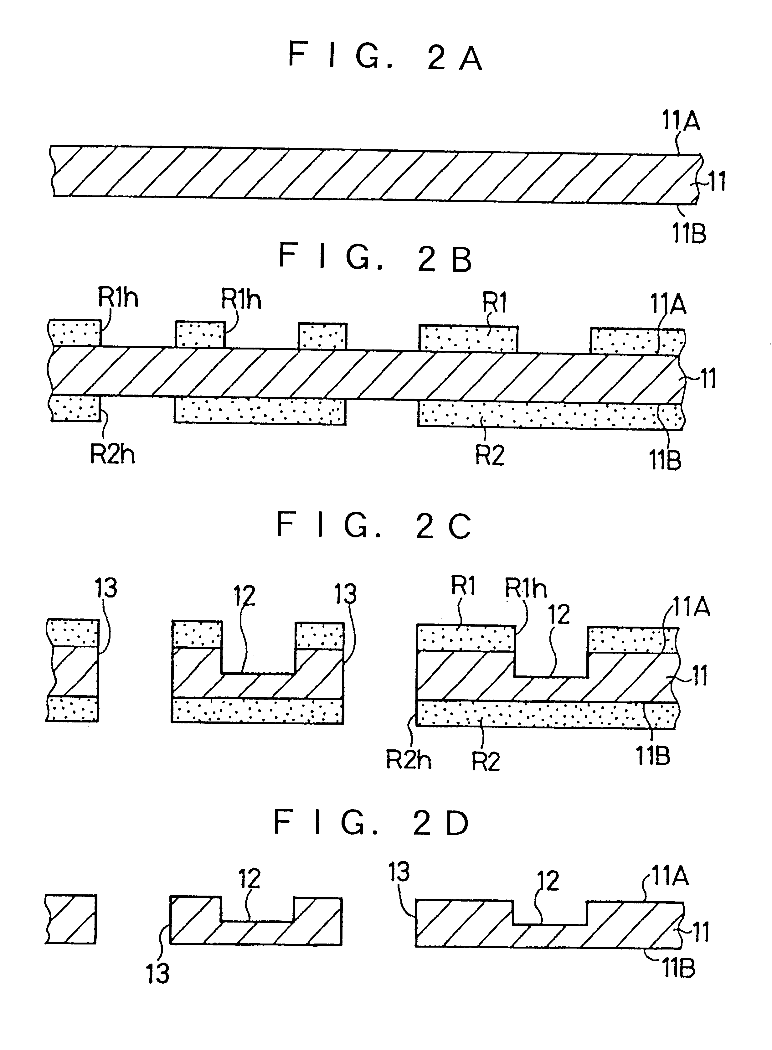
and a via formed on a wall of a through hole for connection to the metal core substrate extending through the insulating resin layers and the metal core substrate so as to establish electrical conductivity to the metal core substrate, wherein the metal core substrate has a thin portion which is thinner than a remaining portion of the metal core substrate; and

the through hole for connection to the metal core substrate is formed through the thin portion.

The through hole for connection to the metal core substrate is preferably formed by...


PUM

PropertyMeasurementUnit
Thicknessaaaaaaaaaa
Electrical conductivityaaaaaaaaaa
Diameteraaaaaaaaaa

Abstract

A multilayer resin wiring board includes a metal core substrate having a first main surface and a second main surface; a plurality of wiring layers located on the first and second main surfaces of the metal core substrate; a plurality of insulating resin layers, each intervening between the metal core substrate and the wiring layers and between the metal core substrate and the wiring layers and between the wiring layers; and a via formed on the wall of a through hole for connection to the metal core substrate extending through the insulating resin layers and the metal core substrate so as to establish electrical conductivity to the metal core substrate. The metal core substrate has a thin portion which is thinner than the remaining portion of the metal core substrate. The through hole for connection to the metal core substrate is formed through the thin portion by laser machining.

Description

1. Field of the InventionThe present invention relates to a multilayer resin wiring board including a metal core substrate, wiring layers, and intervening insulating resin layers, and to a method for manufacturing the same. More particularly, the invention relates to a multilaye resin wiring board including a metal core substrate having a through hole formed thereir and to a method for manufacturing the same.2. Description of the Related ArtMultilayer resin wiring boards are generally known to include alternately-arrranged insulating resin layers and wiring layers and can further include a single or a plurality of metal core substrates. For example, the prior art describes multilayer resin wiring board that include a metal core substrate, insulating resin layers and wiring layers which are alternately arranged on upper and lower sides of the metal core substrate, wherein the metal core substrate of such wiring boards is brought to the grounding potential or a power source potential....

Claims


Application Information

Patent Timeline
IPC IPC(8): H05K3/42H05K3/00H05K3/44H05K3/46B32B15/08B32B15/20H05K1/03
CPCH05K3/0038H05K3/429H05K3/44H05K3/4608Y10T29/49165H05K2201/09554H05K2201/0959H05K2201/09736H05K2201/09745H05K2201/09454
Inventor KAMBE, ROKUROMATSUURA, TORU
Owner NGK SPARK PLUG CO LTD
Learn More