
Amoeba display for hierarchical layout

a hierarchical layout and amoeba technology, applied in the direction of cad circuit design, program control, instruments, etc., can solve the problems of unsatisfactory physical design, unsatisfactory physical design, and undesirable longer wire connection lengths

Inactive Publication Date: 2001-07-03
CADENCE DESIGN SYST INC
View PDF8 Cites 39 Cited by
  • Summary
  • Abstract
  • Description
  • Claims
  • Application Information

AI Technical Summary

Problems solved by technology

Electronic circuit and system designs are becoming increasingly complex, sometimes having over ten million transistors.
Oftentimes, however, design trade-offs arise, for instance, whereupon strictly enforced floor-planning results in undesirable longer wire connection lengths, which translate to physically larger and / or un-route-able layouts as compared to more loosely governed floor-plans.
Hence, more strictly enforced floor-planning approach generally require unduly tedious effort to achieve desired physical design.
Furthermore, in comparison to such strict approach, relatively loose floor-planning, as well as so-called "flat" (i.e., non-hierarchical) automatic placement approaches tend to place components in generally non-hierarchy manner and shape, whereby resulting constraints may generate more route-able placements.

Method used


Image

  • Amoeba display for hierarchical layout
  • Amoeba display for hierarchical layout
  • Amoeba display for hierarchical layout

Examples


2b

15. Case- Add bounding box b to top of perimeter and create n-1 so-called "doughnut-hole" or internal opening perimeters.

16. Else, bounding box b touches more than one existing disjoint perimeter.

17. Case-3: Merge all perimeters to bounding box (i.e., add doughnut holes, if touching bounding box in multiple places).

end

end merge

end.

When operating, present system continually determines list of perimeters by effectively growing or adding to such perimeter list to include instances in given hierarchy from bottom row, then adding instances from next-to-bottom row, and so forth, until all instances in such hierarchy are included therein.

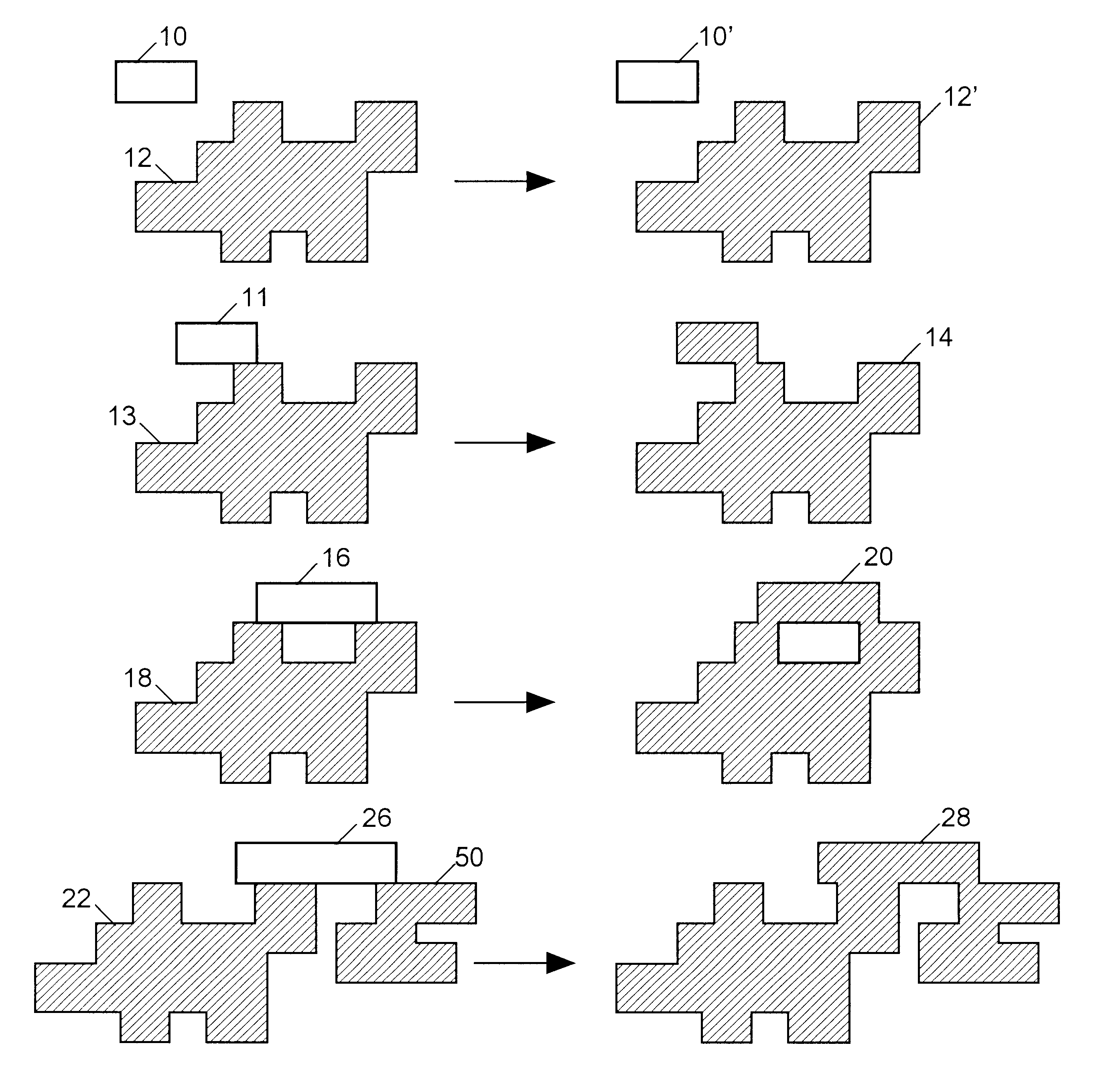
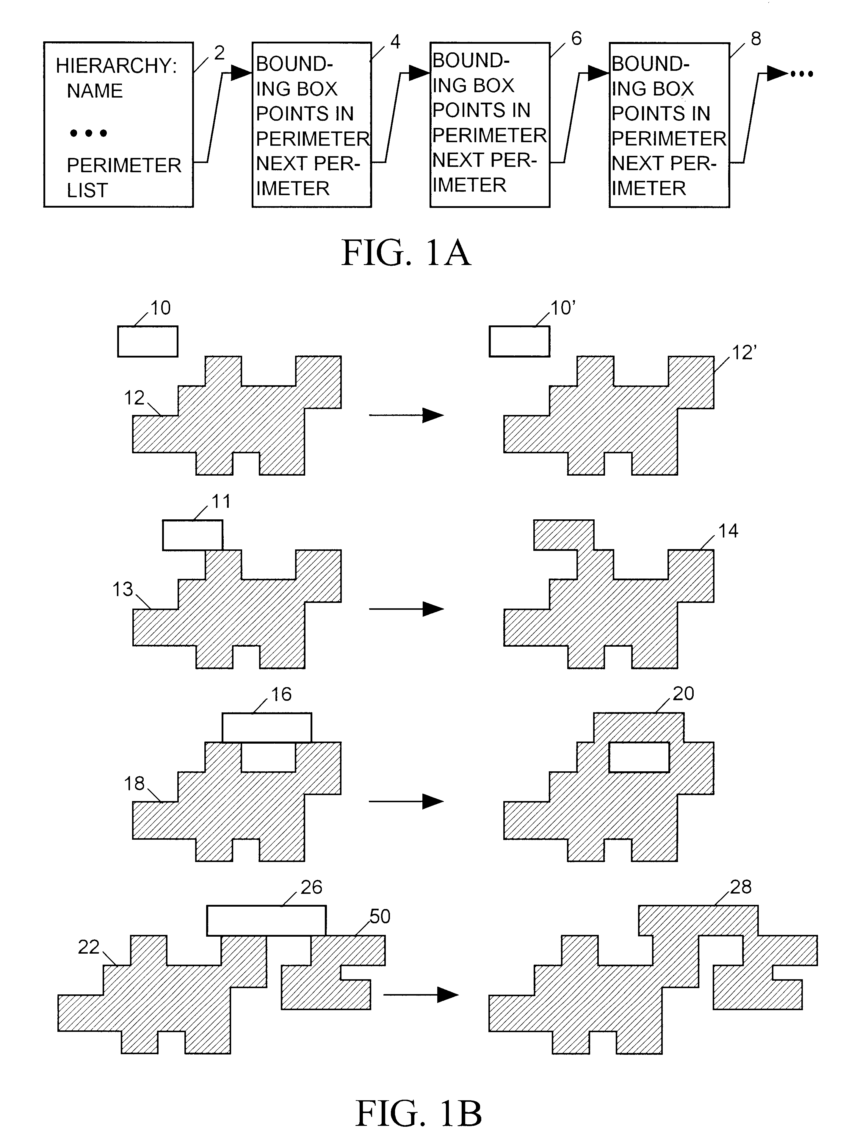
FIG. 1B shows merger of new boxes on top of current perimeter list, for example, illustrating three cases of relationship between new box to be added to perimeter list relative to previously computed perimeter list, both before and after modification of current perimeter list.

Case-1: New box 10 does not touch existing perimeter 12. So, new disjoint perimet...

case-2b

16 touches only one existing perimeter in more than one place. So, new box is merged 20 to existing perimeter, thereby creating doughnut hole.

Case-3: New box 24 touches multiple existing perimeters 22, 26. So, merge perimeters 22, 26 are merged 28 with box 24.

Furthermore, in cleanup phase, after perimeters for hierarchy of design are computed, each perimeter bounding box and sort perimeters are computed in decreasing area, and then reference from hierarchy is saved to sorted perimeter list, as follows:

1. For each perimeter:

2. Save perimeter bounding box.

3. Sort perimeters in decreasing area

4. Set hierarchy cached perimeter list pointer.

Generally, resulting computation of perimeters for hierarchical subcircuit are similar to data structure, as shown in FIG. 1A. Perimeter list data structure for hierarchical subcircuits is illustrated, whereby perimeter list 2 relates hierarchically to next-level bounding box 4, which relates hierarchically to another level bounding box 6, which relat...


PUM


Abstract

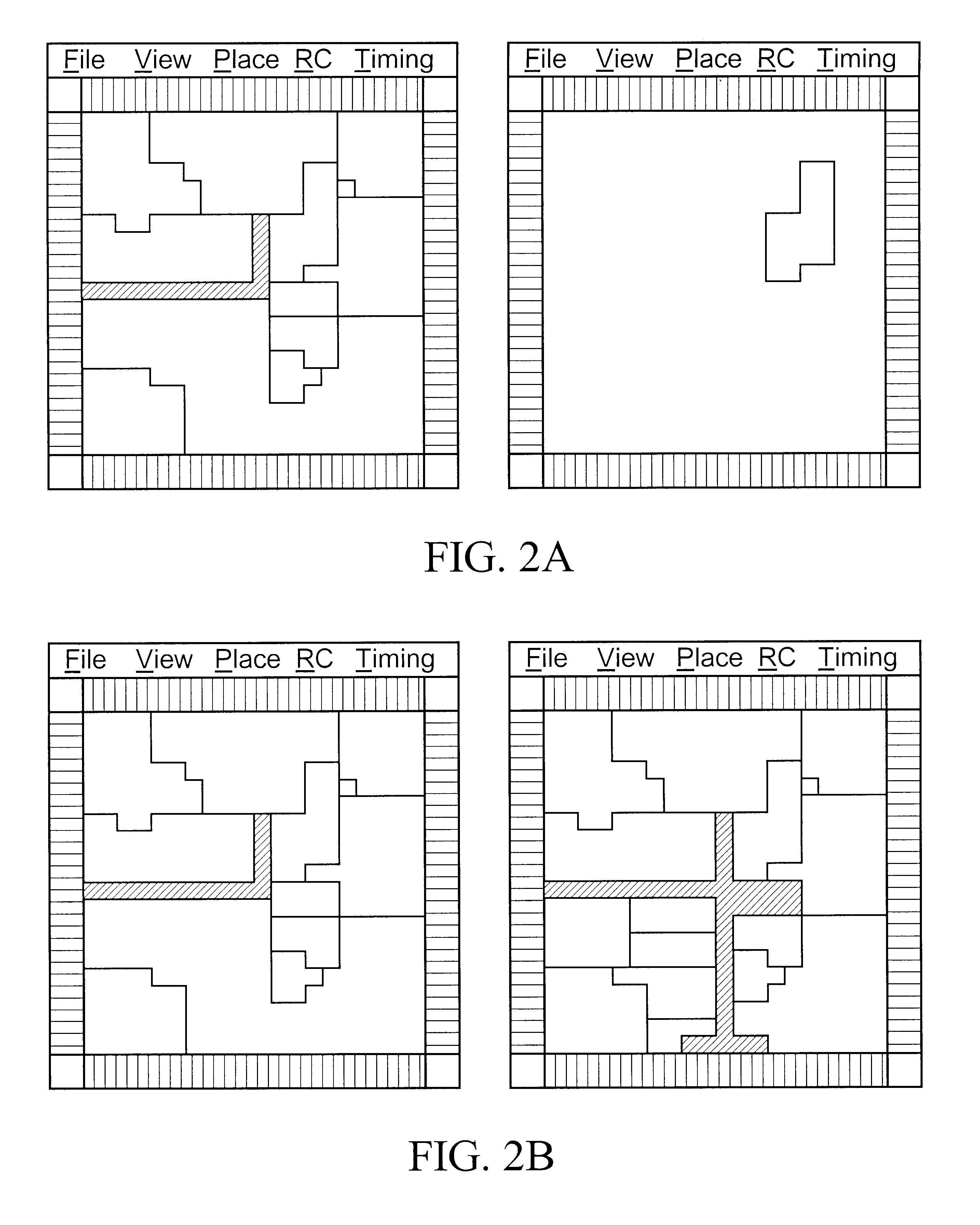
CAD software for automated circuit design provides improved display of hierarchical layout. Component placement perimeters are shown with "amoeba" characteristic for improved circuit floor-planning and analysis. Amoeba view of hierarchical design perimeter enables more intuitive observation of circuit floor-plan from actual component placement. Informational brevity conveyed by perimeters of hierarchies in design facilitates simpler interpretation of complex circuit layout, as well as distributed data access to remote sites through email or low-speed network.

Description

BACKGROUND OF INVENTION1. Field of InventionInvention relates to integrated circuit design, particularly to hierarchical layout display system and methodology for amoeba-type component perimeter placement.2. Description of Background ArtElectronic circuit and system designs are becoming increasingly complex, sometimes having over ten million transistors. To handle such complex magnitude, circuit designs may be represented hierarchically. Furthermore, computer-aided design (CAD) tools facilitate definition and verification of logic-level, as well as physical-level design representations. Additionally, floor-planning and placement steps serve to convert design representation from logical to physical.Floor-planning usually provides "high-level" block (i.e., rectangular) diagram representing hierarchical logic design, wherein such blocks may represent top or child-level components in design hierarchy. Moreover, automated placement tools may use floor-planning to provide "strict" or "loo...

Claims


Application Information

Patent Timeline
Patent Type & Authority Patents(United States)
IPC IPC(8): G06F17/50
CPCG06F17/5068G06F30/39
Inventor IGUSA, MITSURU
Owner CADENCE DESIGN SYST INC
Learn More