Memory device
- Summary
- Abstract
- Description
- Claims
- Application Information
AI Technical Summary
Benefits of technology
Problems solved by technology
Method used
Image

Examples
first embodiment
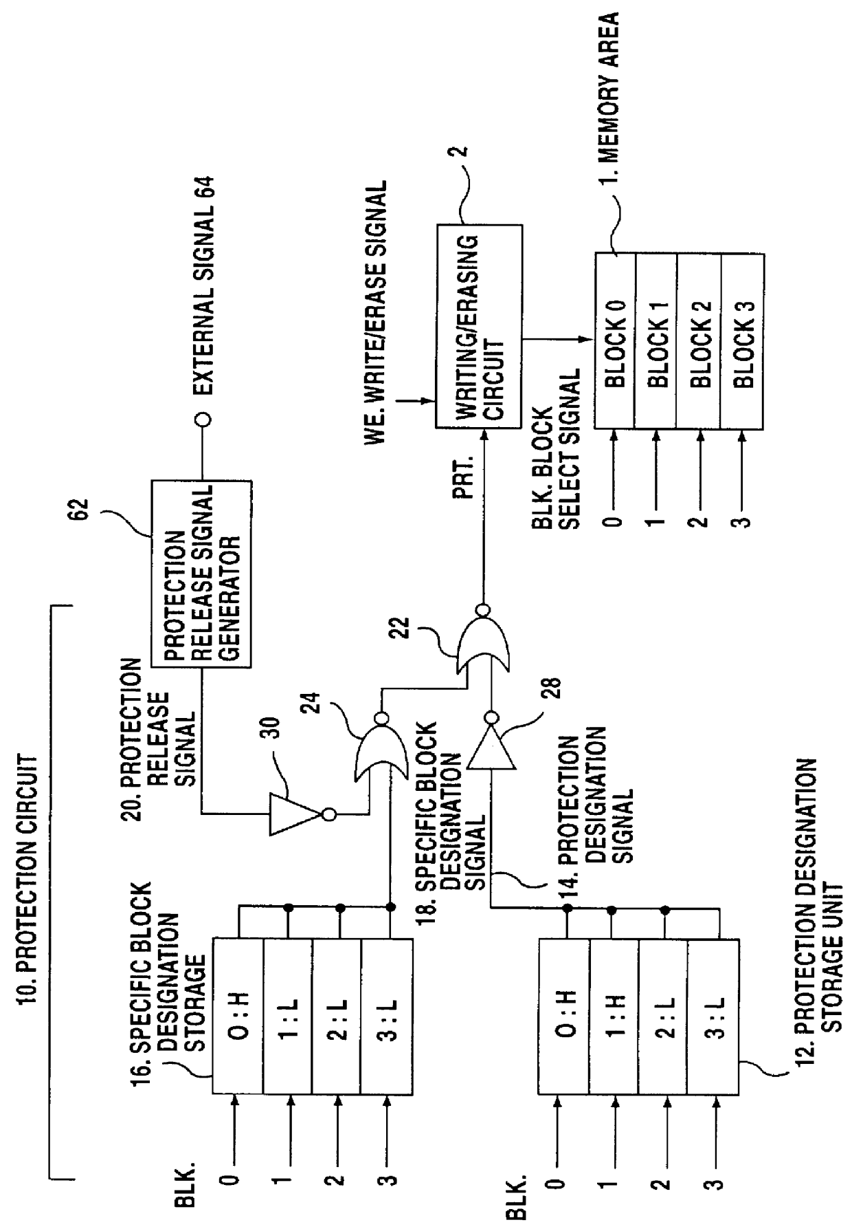
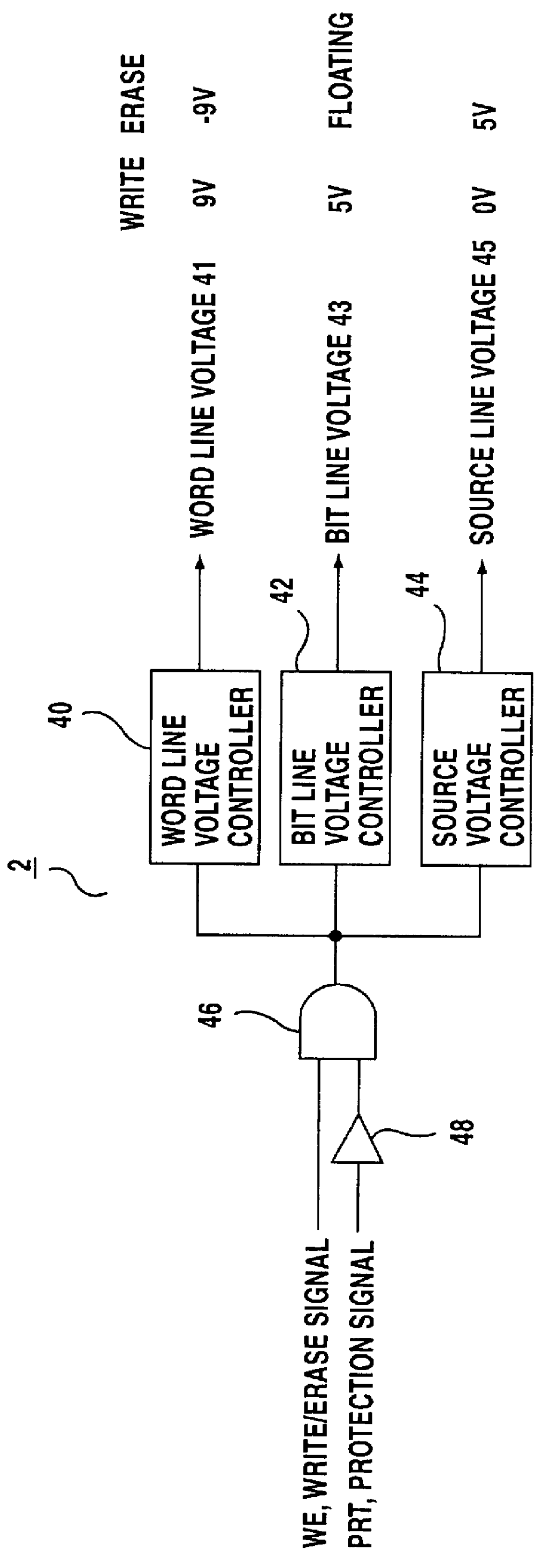
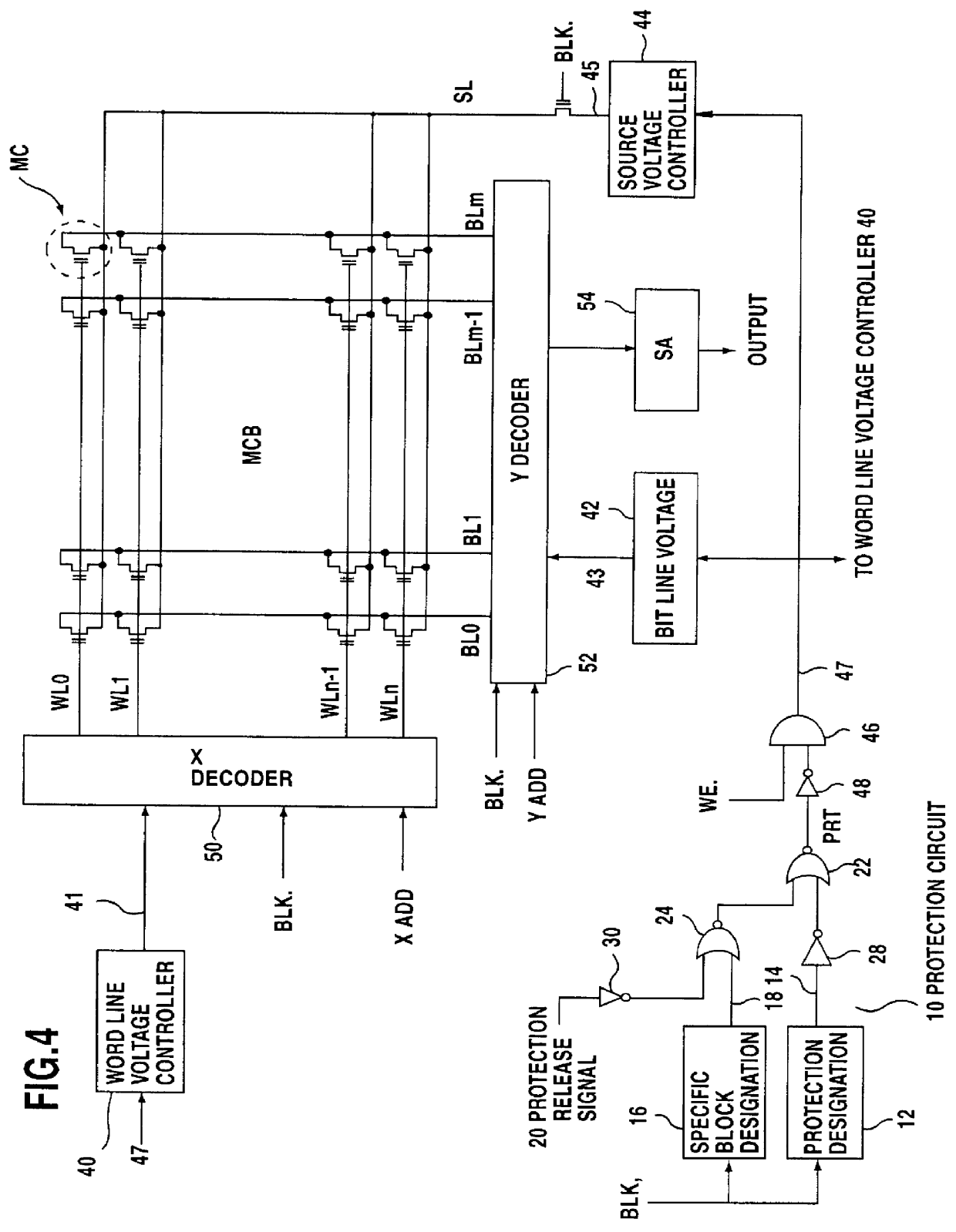
FIG. 1 is a diagram illustrating a protection circuit arrangement according to the present invention. In FIG. 1, a memory area 1 consists of four memory blocks, 0 to 3. One of the memory blocks 0 to 3 is selected in accordance with a block select signal BLK, and writing (of a program), erasing and reading processes are performed for the selected memory block. A plurality of memory cells, which are nonvolatile memory cells, as will be described later, are provided for each of the memory blocks which constitute the memory area 1. The general structure of a nonvolatile memory cell includes a control gate connected to a word line, a drain electrode connected to a bit line, a source electrode connected to a source line, and a floating gate used for the storage of data. To write data (a program) into the nonvolatile memory cell, for example, it is set to a condition wherein the word line voltage is 9 V, the bit line voltage is 5 V and the source voltage is 0 V, so that electrons are intro...
case 2
In case 2 in FIG. 9, the first protection release signal 20 is in the released state (level H) and the second protection release signal 60 is in the unreleased state (level L). In case 2, the writing and the erasing of data in memory blocks other than a specific block is permitted. As for a specific block, either the protection is released or the protection is forcibly set in accordance with the protection designation signal 14. In other words, this corresponds to cases 3 to 6 in FIG. 2 or in the modification in FIG. 6.
In cases 3 and 4 in FIG. 9, the second protection release signal 60 is in the released state (level H). In these cases, regardless of the first protection release signal 20 and of the state of the protection designation signal 14 which is output from the protection designation storage unit 12, the protection of data in all of the memory blocks is released, and the protection signal PRT is forcibly set to the unprotected state (level L). As a result, the writing and th...
second embodiment
As is described above, when the first and the second protection release signals 20, 60 are in the unreleased state, the state of the protection signal PRT is determined in accordance with the protection designation signal 14, which is output from the protection designation storage unit 12. In addition, when the first protection release signal 20 is set to the released state (level L), the state of the protection signal PRT is determined in accordance with the specific block designation signal 18 output by the specific block designation storage unit 16, and the data in a specified memory block are protected. When the second protection release signal 60 is set to the released state (level H), the protection signal PRT is set to the unprotected state (level L), even if a block is specified, and the writing and the erasing of data in all of the memory blocks is permitted.
In the first and the second embodiments, the protection release signals 10 and 60 are generated by using a received ...
PUM
 Abstract
Description
Claims
Application Information
 - R&D
- Intellectual Property
- Life Sciences
- Materials
- Tech Scout
- Unparalleled Data Quality
- Higher Quality Content
- 60% Fewer Hallucinations
Browse by: Latest US Patents, China's latest patents, Technical Efficacy Thesaurus, Application Domain, Technology Topic, Popular Technical Reports.
© 2025 PatSnap. All rights reserved.Legal|Privacy policy|Modern Slavery Act Transparency Statement|Sitemap|About US| Contact US: help@patsnap.com