
Apparatus and method for automatically loading or unloading printed circuit boards for semiconductor modules

a technology of printed circuit boards and automatic loading, applied in the direction of packaging goods, charge manipulation, furniture, etc., can solve the problems of failure of pcbs to be subjected to the final steps of the process, waste of sheet-type pcbs, and raised problems with use of sheet-type pcbs

Inactive Publication Date: 2000-05-16
INTELLECTUAL DISCOVERY CO LTD
View PDF11 Cites 56 Cited by
  • Summary
  • Abstract
  • Description
  • Claims
  • Application Information

AI Technical Summary

Problems solved by technology

However, the use of the sheet-type PCBs raises some problems.
One problem is that the sheet-type PCBs include wasted parts, such as link parts or space.
Moreover, although unexpected failure may be found among the individual PCBs composing one sheet-type PCB during the manufacturing process, the failed PCBs are subjected to the final steps of the process because of the difficulty in removing the failed PCBs.
This can significantly reduce productivity.
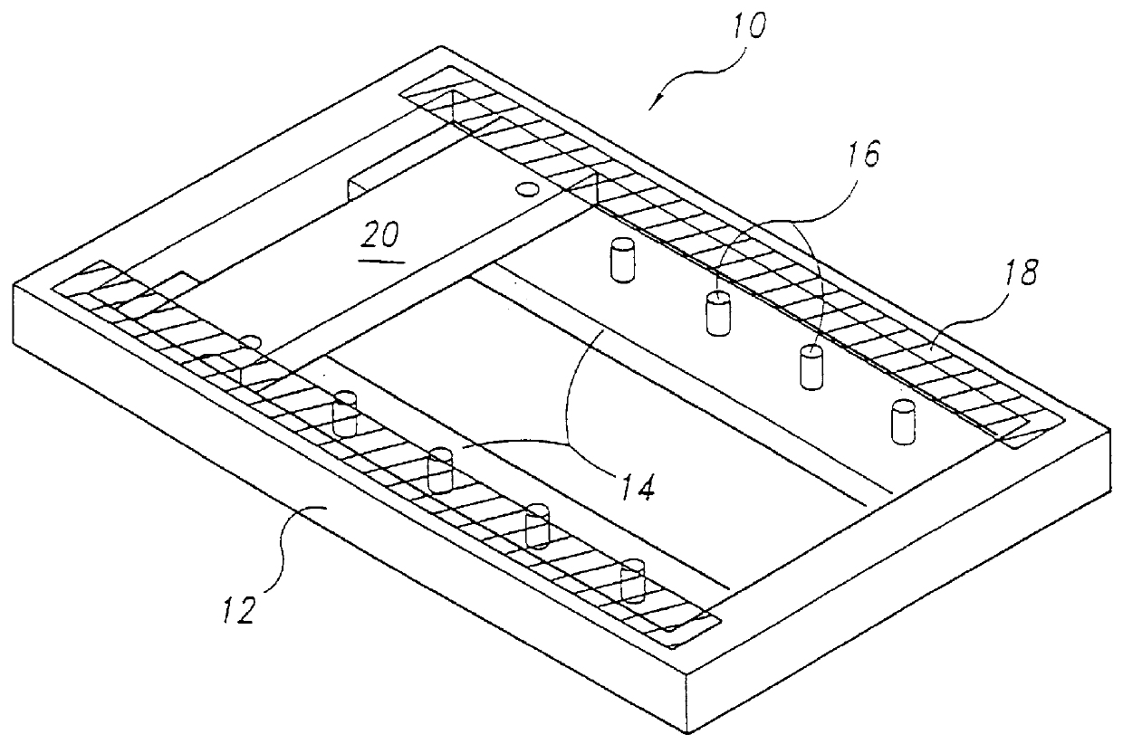
A disadvantage of the existing jig carrier 10 is that attaching the tape 18 and the loading of the PCBs 20 are done manually.
The required manual manipulations reduce the productivity of the module manufacturing process.

Method used


Image

  • Apparatus and method for automatically loading or unloading printed circuit boards for semiconductor modules
  • Apparatus and method for automatically loading or unloading printed circuit boards for semiconductor modules
  • Apparatus and method for automatically loading or unloading printed circuit boards for semiconductor modules

Examples


Embodiment Construction

The present invention will now be described more fully hereinafter with reference to accompanying drawings, in which preferred embodiments of the invention are shown. This invention may, however, be embodied in many different forms and should not be construed as limited to the embodiments set forth herein.

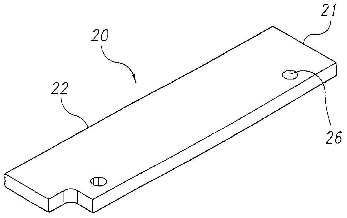
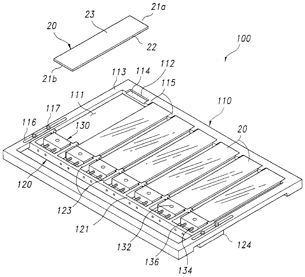
FIG. 3 is a perspective view of a jig carrier 100 employed to carry a plurality of printed circuit boards (PCBs) 20 for semiconductor modules. Referring to FIG. 3, each of the PCBs 20, which are carried by the jig carrier 100, has two opposite plane surfaces 23, two opposite shorter edges 21a and 21b, and two opposite longer edges 22. The jig carrier 100 permits automatic loading or unloading processes of the present invention, as will be described later.

The jig carrier 100 comprises a rectangular main frame 110, a clamp frame 120 and at least one clamps 130, preferably of the same number as the PCBs 20. The main frame 110 is formed with an inside space 111 for the PCBs 20. When th...


PUM


Abstract

An apparatus for automatic loading or unloading printed circuit boards (PCBs) for semiconductor modules is disclosed. The apparatus employs an elastic jig carrier into which the PCBs are loaded. The jig carrier includes movable clamps for fixing the PCBs by elastic force. A jig opener of the apparatus applies opening force, in the reverse direction of the elastic force, to the movable clamps so that the PCBs can be loaded into or unloaded from the jig carrier by a picker. The jig carrier is transferred along a conveyor belt, while the PCBs are supplied from a PCB stage such as a tray to the jig carrier. The apparatus may further comprise a gripper and a rotator. The gripper grips the upright PCBs and the rotator rotates them to be horizontal, so that the picker can pick up the horizontal PCBs. The apparatus may also comprise an aligner for exact alignment of the PCBs in the jig carrier. A method for loading or unloading the PCBs into or from the jig carrier is also disclosed in connection with the apparatus.

Description

1. Field of the InventionThe present invention relates generally to an apparatus and a method employed in manufacture of semiconductor modules. More particularly, the present invention relates to automatically loading or unloading multiple printed circuit boards into or from a jig carrier during a process of manufacturing semiconductor modules.2. Description of the Prior ArtAs electronic devices become more complex and employ more integrated circuits, it is desirable, if possible, to avoid increasing the space they occupy. To solve this problem, modules mounted with multiple integrated circuit devices have been employed. In a typical module, the integrated circuit devices, for example, semiconductor packages, are attached to either one side of a printed circuit board (PCB) in case of a single-sided module or both sides of PCB in case of a double-sided module.For higher productivity, modules are generally produced in a production line where PCBs move along conveyor belt. In particula...

Claims


Application Information

Patent Timeline
Patent Type & Authority Patents(United States)
IPC IPC(8): H05K7/14
CPCH05K7/1415
Inventor HAN, SEONG CHANLEE, DONG CHUNYU, KWANG SUKWON, O KYUNG
Owner INTELLECTUAL DISCOVERY CO LTD
Learn More