
Display device

a display device and display technology, applied in the direction of identification means, semiconductor devices, instruments, etc., can solve the problems of weak immersion and weak sense of reality

Pending Publication Date: 2022-06-30
SEMICON ENERGY LAB CO LTD
View PDF0 Cites 2 Cited by
  • Summary
  • Abstract
  • Description
  • Claims
  • Application Information

AI Technical Summary

Benefits of technology

The patent aims to provide a display device with high resolution, low power consumption, high luminance, a high aperture ratio, and high reliability. Additionally, it aims to provide a novel display device, display module, and electronic device that can overcome the limitations of conventional techniques. The patent also includes a method for manufacturing the display device with high yield. The technical effect of the patent is to improve display quality and performance while reducing power consumption and manufacturing costs.

Problems solved by technology

Since part of the screen is enlarged by the lens, low resolution of the display panel might cause a problem of weak sense of reality and immersion.

Method used


Image

  • Display device
  • Display device
  • Display device

Examples


embodiment 1

[0067]In this embodiment, a structure example of a display device of one embodiment of the present invention will be described.

[0068]One embodiment of the present invention is a display device that includes a plurality of pixels arranged in a matrix. The display device includes a plurality of source lines (first wirings) supplied with source signals (also referred to as video signals, data signals, or the like) and a plurality of gate lines (second wirings) supplied with gate signals (also referred to as scan signals or the like). The source lines extend in a first direction, and the gate lines extend in a second direction that intersects the first direction.

[0069]Each pixel is provided for the intersection portion of one source line and one gate line. The pixel includes one or more display elements and one or more transistors. The pixel includes a pixel electrode functioning as an electrode of the display element.

[0070]When electrical noise that is caused by a signal supplied to th...

structure example 1

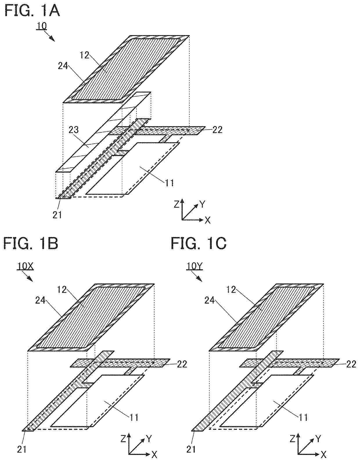
[0077]FIG. 1A is a schematic perspective view illustrating a stacked-layer structure of one of subpixels of a display device 10. The subpixel includes a pixel circuit 11, a light-emitting element 12, a wiring 21, a wiring 22, and a wiring 23. The light-emitting element 12 includes a pixel electrode 24.

[0078]The wiring 21 functions as a source line and extends in a Y direction. The wiring 22 functions as a gate line and extends in an X direction. The wiring 23 is supplied with a constant potential and includes a portion extending in the Y direction.

[0079]The light-emitting element 12 is provided in the inside of the pixel electrode 24. As the light-emitting element 12, for example, an electroluminescence element in which a layer containing a light-emitting substance (also referred to as an EL layer) is interposed between a pair of electrodes is suitably used. The electroluminescence element emits light when current flows between the pair of electrodes. In particular, an organic EL el...

structure example 2

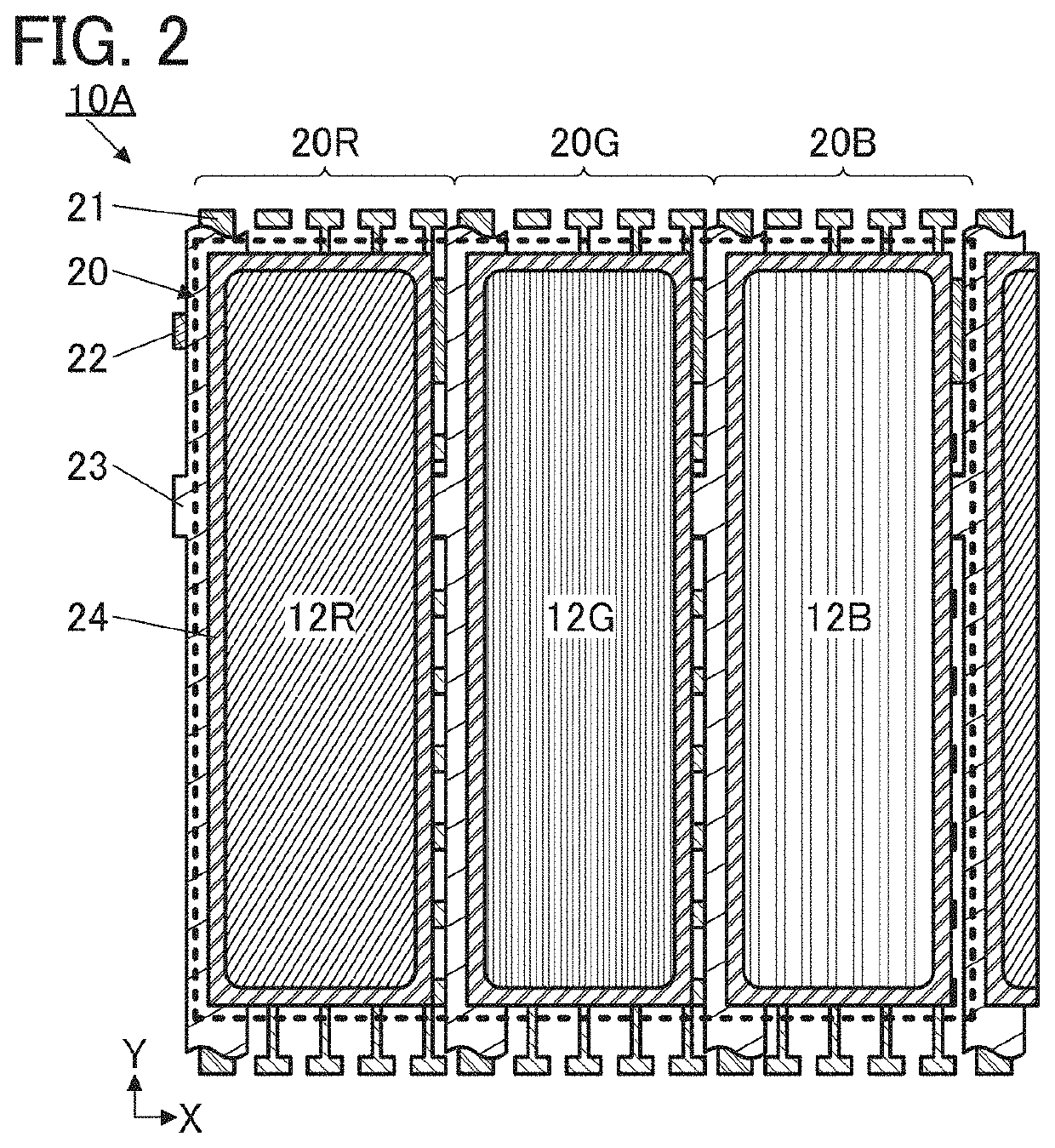
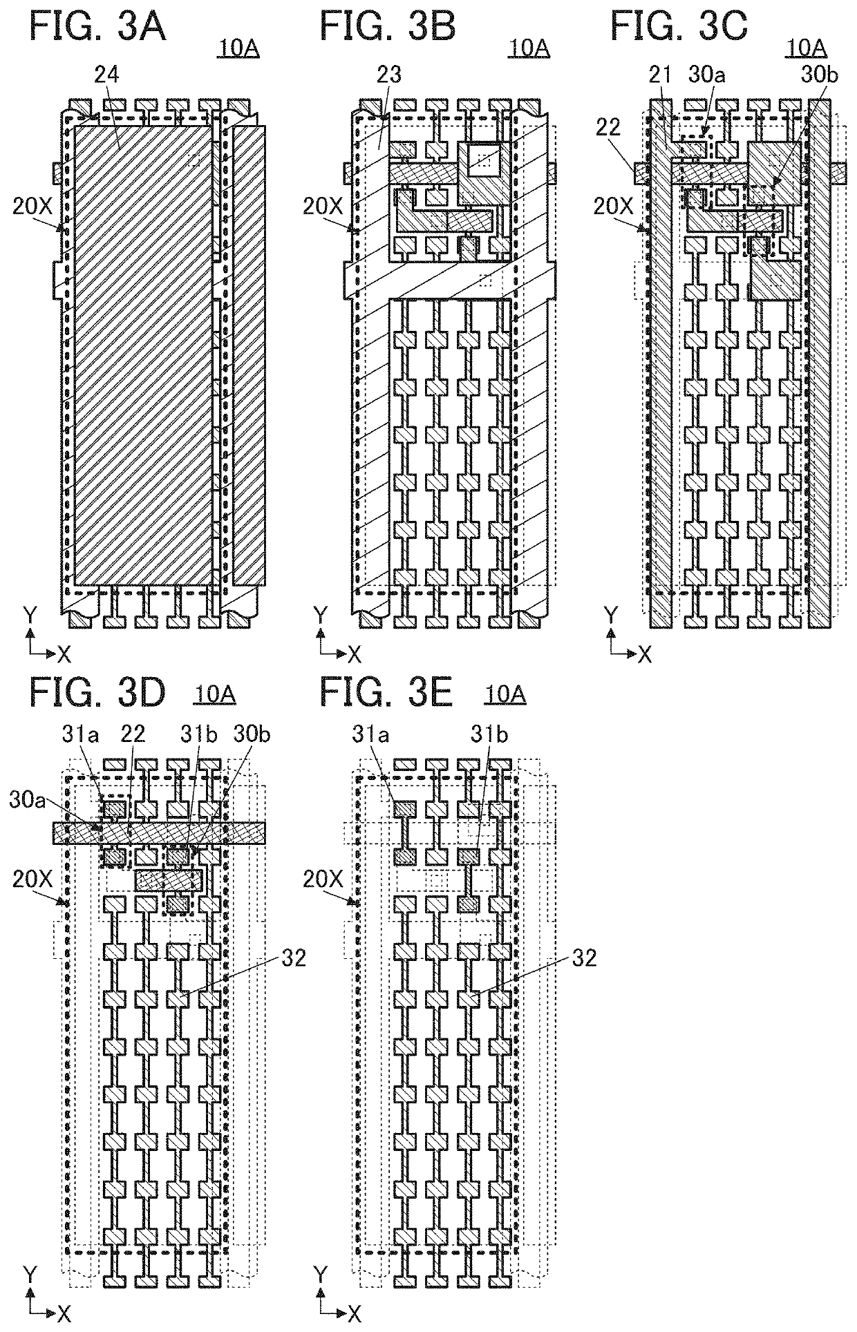
[0086]A more specific structure example of the pixel will be described below.


PUM


Abstract

A display device with high resolution is provided. A display device with low power consumption is provided. A display device with high luminance is provided. A display device with a high aperture ratio is provided. The display device includes a first wiring, a second wiring, a third wiring, and a pixel electrode. The first wiring extends in a first direction and is supplied with a source signal. The second wiring extends in a second direction intersecting the first direction and is supplied with a gate signal. The third wiring is supplied with a constant potential. The first wiring and the pixel electrode overlap with each other with the third wiring therebetween.

Description

BACKGROUND OF THE INVENTION1. Field of the Invention[0001]One embodiment of the present invention relates to a display device. One embodiment of the present invention relates to an electronic device including a display device.[0002]Note that one embodiment of the present invention is not limited to the above technical field. Examples of the technical field of one embodiment of the present invention disclosed in this specification and the like include a semiconductor device, a display device, a light-emitting apparatus, a power storage device, a memory device, an electronic device, a lighting device, an input device, an input / output device, a driving method thereof, and a manufacturing method thereof. A semiconductor device refers to a device that can function by utilizing semiconductor characteristics in general.2. Description of the Related Art[0003]In recent years, the resolution of a display panel has been increased. As a device that requires a high-resolution display panel, a de...

Claims


Application Information

Patent Timeline
IPC IPC(8): H01L27/32H01L29/786
CPCH01L27/3276H01L29/78651H01L29/78696H01L29/78618G09F9/30G09F9/33H10K59/121H10K59/1213H10K59/131H01L27/124H01L27/1225H10K59/00
Inventor KOBAYASHI, HIDETOMOSHISHIDO, HIDEAKIKATSUI, SHUICHI
Owner SEMICON ENERGY LAB CO LTD
Learn More